Liquid crystal display apparatus

a technology of liquid crystal display and display device, which is applied in the direction of identification means, instruments, non-linear optics, etc., can solve problems such as delay in respons

Inactive Publication Date: 2002-03-21
GOLD CHARM LTD
View PDF0 Cites 66 Cited by
  • Summary
  • Abstract
  • Description
  • Claims
  • Application Information

AI Technical Summary

Problems solved by technology

Consequently, because the director rotates within the substrate surface in this display system, the problem that a relationship between the light transmission quantity and the voltage application quantity in the case of TN system, when watching in the direction of the director and in the direction of normal of the substrate has a large difference, does not occur, then it is possible to obtain good picture while watching from very wide angle of vision.
However, in the conventional IPS system of liquid crystal display apparatus, there is a problem that the pixel electrodes and the common elec

Method used


Image

  • Liquid crystal display apparatus
  • Liquid crystal display apparatus
  • Liquid crystal display apparatus

Examples


first embodiment

[0055] [First Embodiment]

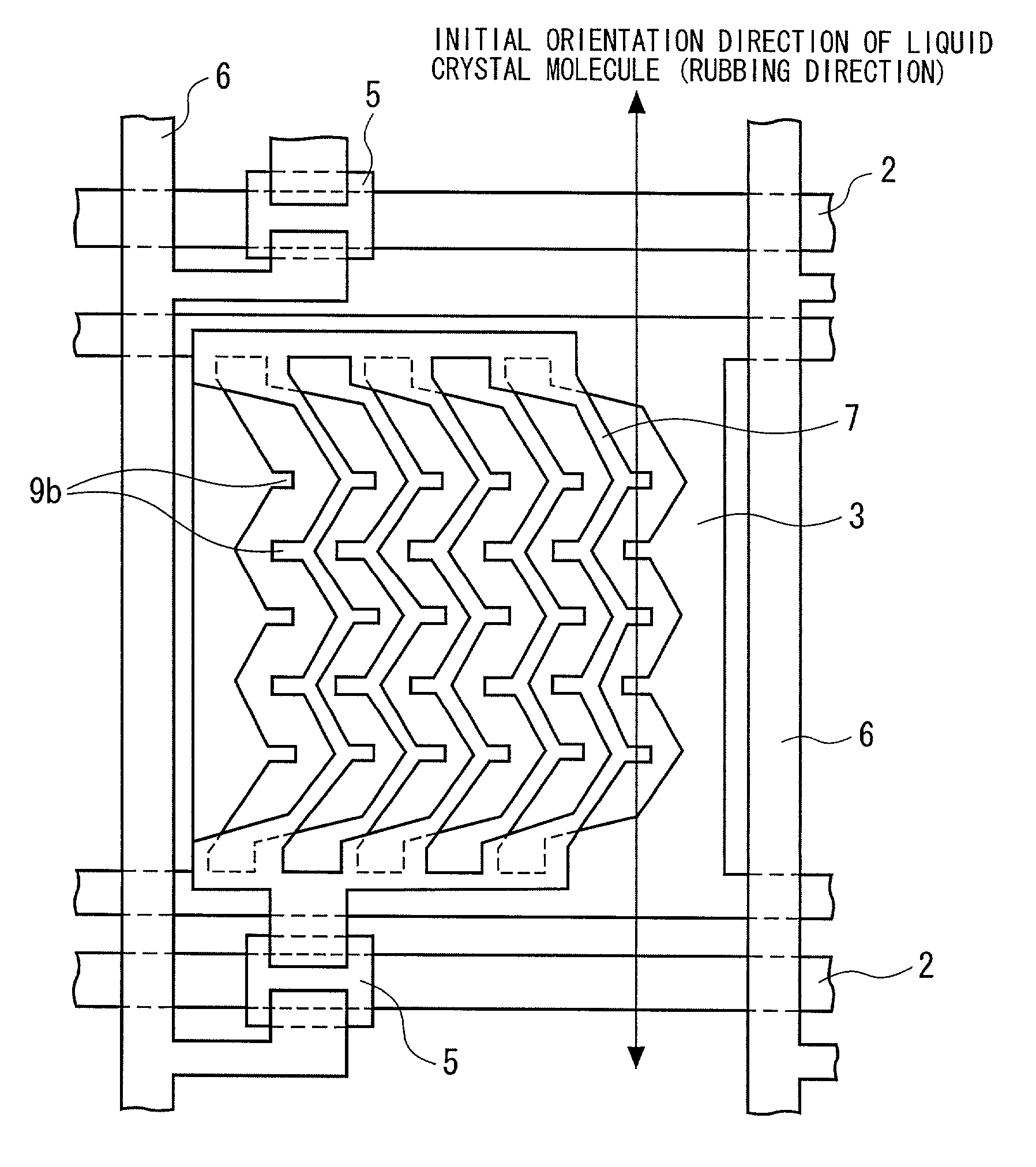
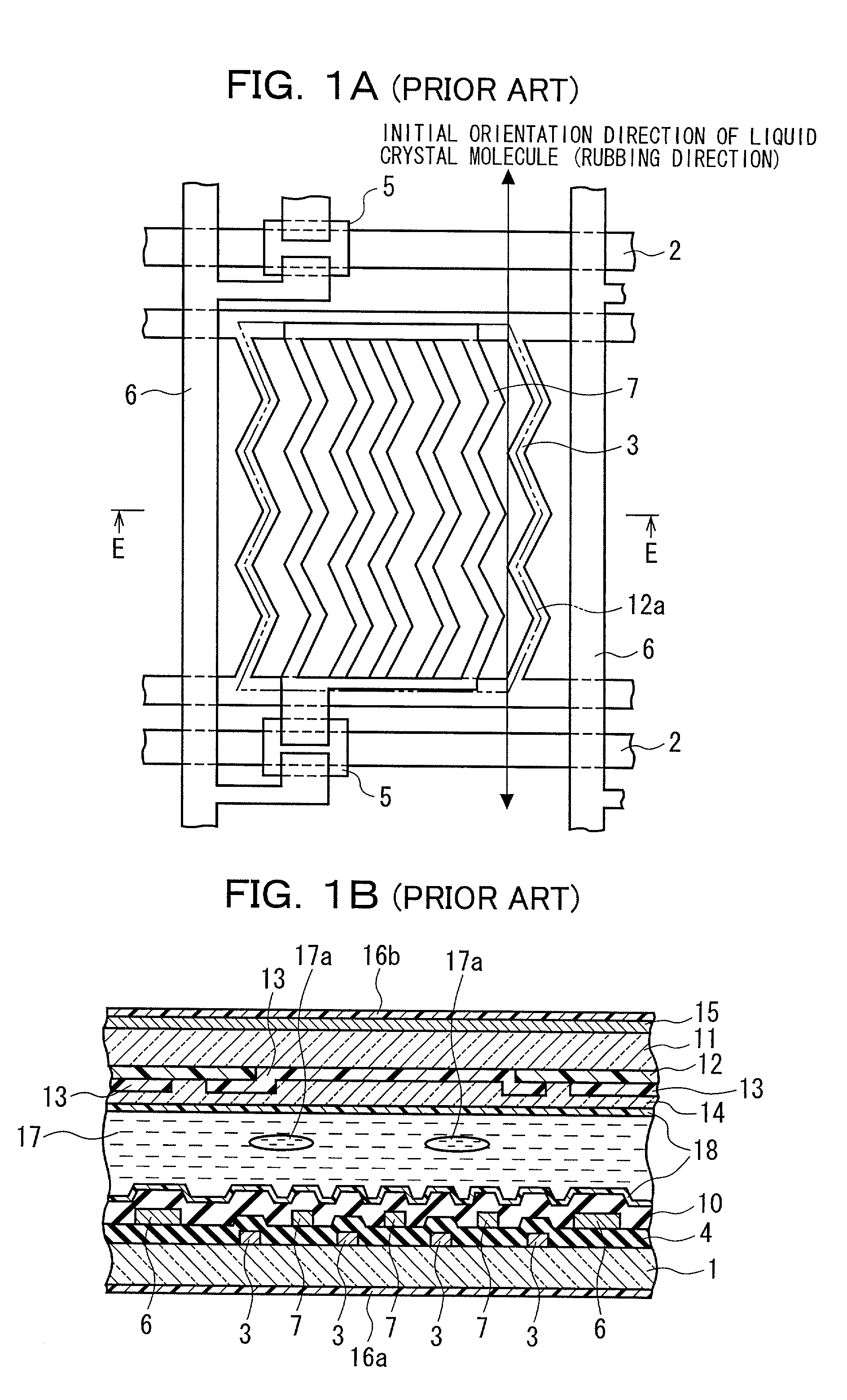
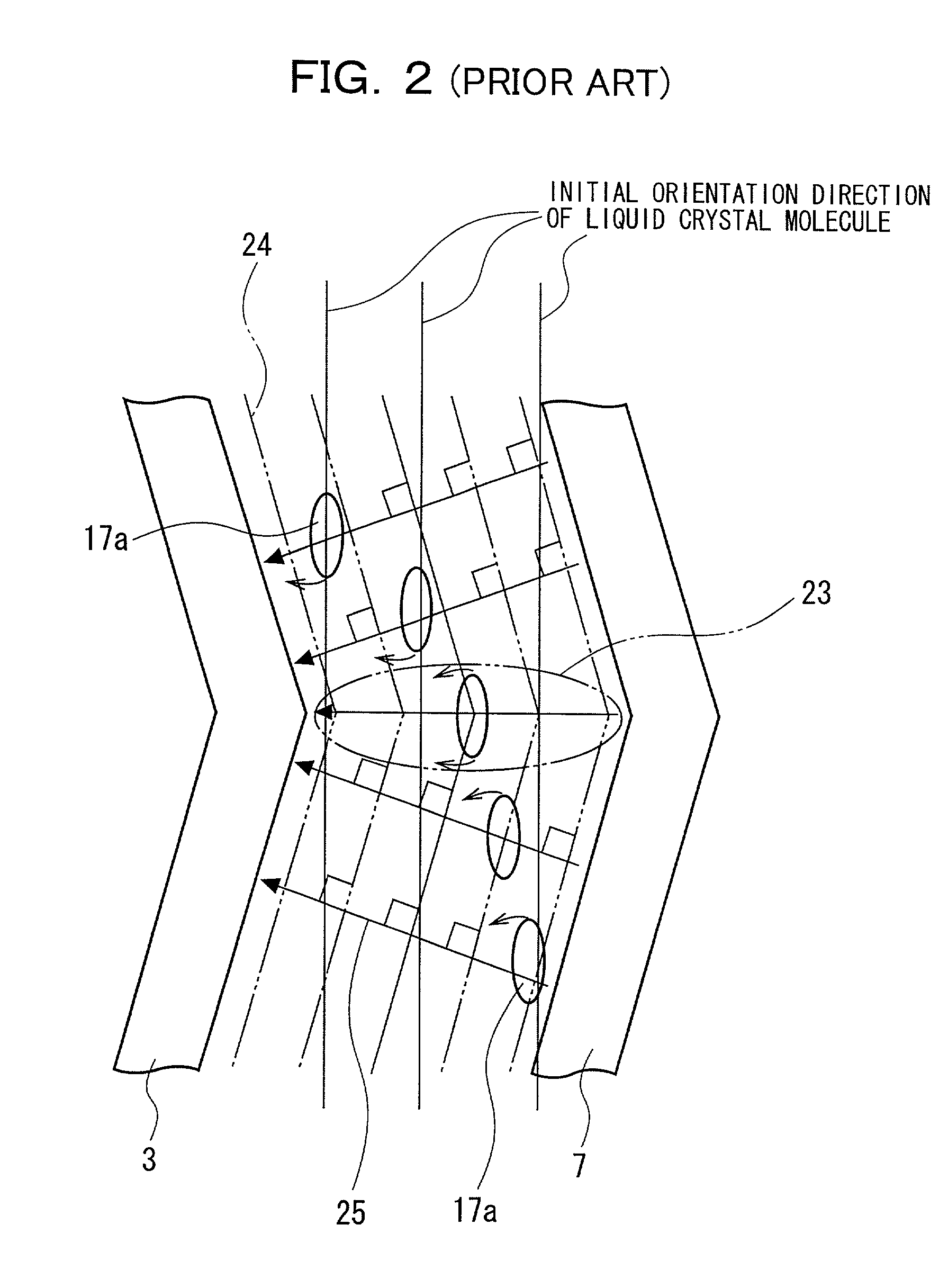
[0056] The IPS system liquid crystal display apparatus according to the first embodiment of the present invention will be described referring to FIG. 3 to FIG. 12. FIG. 3 is a plan view illustrating a structure of a liquid crystal display apparatus according to a first embodiment of the present invention. FIG. 4 is a view schematically illustrating process order of manufacturing method of the liquid crystal display apparatus according to the first embodiment of the present invention, FIG. 4A is a plan view, and FIG. 4B is a sectional view along line A-A of FIG. 4A. FIG. 5 is a view schematically illustrating process order of manufacturing method of the liquid crystal display apparatus according to the first embodiment of the present invention, FIG. 5A is a plan view, and FIG. 5B is a sectional view along line B-B of FIG. 5A. FIG. 6 is a view schematically illustrating process order of manufacturing method of the liquid crystal display apparatus according to ...

second embodiment

[0072] [Second Embodiment]

[0073] Next, IPS system liquid crystal display apparatus according to the second embodiment of the present invention will be described referring to FIGS. 13A and 13B. FIGS. 13A and 13B are plan views illustrating unit pixel formed by adjacent pixel electrode and common electrode. FIG. 13A illustrates a case that the number of bent point is one, and FIG. 13B illustrates a case that the number of bent point is three. The present embodiment describes about technique for optimizing shape of the projected section 9b and the number of bent point from the viewpoint of the aperture rate.

[0074] Namely, although it is possible to plan improvement of the visual angle characteristic when increasing the number of bent point, in cases where respective bent sections 9a of the pixel electrode 7 and the common electrode 3 are provided with the projected section 9b, decrease of the aperture rate caused by the fact that light of the opening section is shaded by the projected ...

third embodiment

[0083] [Third Embodiment]

[0084] Next, IPS system liquid crystal display apparatus according to the third embodiment of the present invention will be described referring to FIGS. 14A to 14C. FIGS. 14A to 14C are sectional views illustrating structure of TFT side substrate of the liquid crystal display apparatus according to the third embodiment. The present embodiment describes about a structure and method for reducing scraps of the orientation film that are formed on the occasion of the rubbing treatment of the orientation film, constitution of the other parts is the same as that of the first and the second embodiments.

[0085] As illustrated in FIGS. 14A to 14C, in the TFT side substrate of the liquid crystal display apparatus formed the gate line 2 and the common electrode 3 on the first transparent substrate 1, the signal line 6 and the pixel electrode 7 are formed thereon through the interlayer isolation film 4 made of the silicon oxide film 4a, silicon nitride film 4b and so fort...


PUM


Abstract

A liquid crystal display apparatus has a pair of substrates opposing to each other and a liquid crystals sandwiched between the pair of substrates. One side of substrate is provided with gate lines and signal lines which approximately cross each other. TFTs are provided close to intersection portion of the gate line and the signal line. Pixel electrodes and common electrodes are provided at each pixel enclosed by the gate line and the signal line. Each of pixel electrodes and common electrodes has bent points more than one and is alternately formed in parallel with each other. Both the pixel electrode and the common electrode are made up of bent sections and projected sections projecting toward concave sections of opposite electrodes from convex side top sections of the bent sections. In the liquid crystal display apparatus, improvement of visual angle characteristics and response characteristics is planned in such a way that the projected section allows electric field close to the bent section to be stabilized, and allows electric field strength to be enhanced.

Description

[0001] 1. Field of the Invention[0002] The present invention relates to a liquid crystal display apparatus, and more particularly to a liquid crystal display apparatus of IPS (In-Plane Switching) system in which liquid crystal is made to drive within a surface approximately parallel to a TFT (Thin Film Transistor) substrate by applying a voltage to a pixel electrode and a common electrode therebetween formed on the TFT substrate.[0003] 2. Description of the Related Art[0004] An active matrix type liquid crystal display apparatus, having a picture quality of high dignity, uses a thin film transistor (hereinafter referred to TFT) as a switching element of pixels, and is widely used as space-saving designed monitor of a desktop computer and so forth. Generally, in the operating mode of the liquid crystal display apparatus, there are two systems of Twisted Nematic: TN system which allows direction of directors of oriented liquid crystal molecules to be rotated in the perpendicular direc...

Claims


Application Information

Patent Timeline
IPC IPC(8): G02F1/137G02F1/1337G02F1/1343G02F1/139G09F9/30
CPCG02F1/134363G02F1/1343
Inventor HIDEHIRA, MASANOBUWATANABE, MAKOTOKUROHA, SYOUICHI
Owner GOLD CHARM LTD
Why Eureka
Try Eureka