
Electrically erasable, programmable, non-volatile memory device compatible with a cmos/soi production process

a non-volatile memory, programmable technology, applied in the direction of semiconductor devices, electrical apparatus, transistors, etc., can solve the problems of limited type of memory cells and tunnel oxide reliability problems

Inactive Publication Date: 2002-04-04
COMMISSARIAT A LENERGIE ATOMIQUE ET AUX ENERGIES ALTERNATIVES
View PDF0 Cites 10 Cited by
  • Summary
  • Abstract
  • Description
  • Claims
  • Application Information

AI Technical Summary

Benefits of technology

[0012] The dielectric insulation of the components obtained as a result of the insulation zones is of a total nature and makes it possible to reduce to the minimum the insulation distance between the transistors, in a device having several memory cells.
[0015] The storage device according to the invention solely uses transistors of a single conductivity type in the memory plane, no matter whether they are storage or selection transistors. This leads to a simplification in the production processes compared with a NMOS and PMOS memory cell requiring a dual N.sup.+ and P.sup.+ gate.
[0016] The total dielectric insulation of the control gate implemented in diffusion makes it possible to use a control voltage of random sign (positive or negative), as well as high control voltage values without any risk of latch-up or electric leaks.

Problems solved by technology

Despite an interesting functionality and a current use of this type of memory cell in the implementation of integrated circuits, this type of memory cell is limited as regards the integration density, bearing in mind its large surface area (cell size approximately 100 .mu.m.sup.2 for a 1.2 .mu.m technology and 70 .mu.m for a 0.7 .mu.m technology).
Moreover, as in double poly EEPROMs, this type of structure suffers from a tunnel oxide reliability problem linked with the large surface of the tunnel oxide zone.

Method used


Image

  • Electrically erasable, programmable, non-volatile memory device compatible with a cmos/soi production process
  • Electrically erasable, programmable, non-volatile memory device compatible with a cmos/soi production process
  • Electrically erasable, programmable, non-volatile memory device compatible with a cmos/soi production process

Examples


Embodiment Construction

[0007] The present invention relates to a non-volatile memory cell, e.g. of the electrically bit by bit programmable and erasable EEPROM type and having the special feature of being conventionally implementable in a CMOS / SOI process. In addition, the memory cell surface area is preferably small.

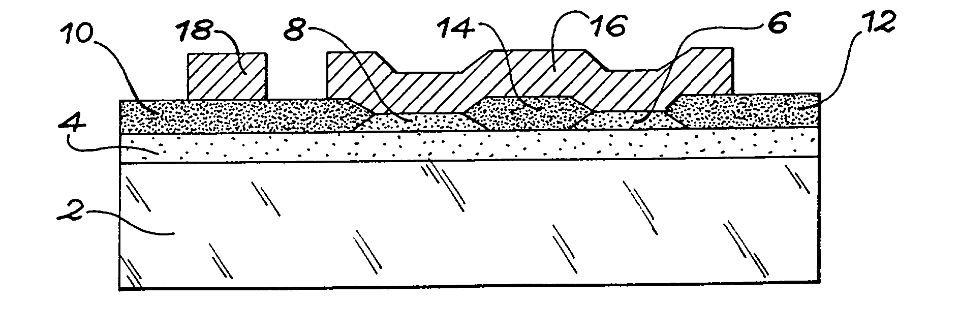
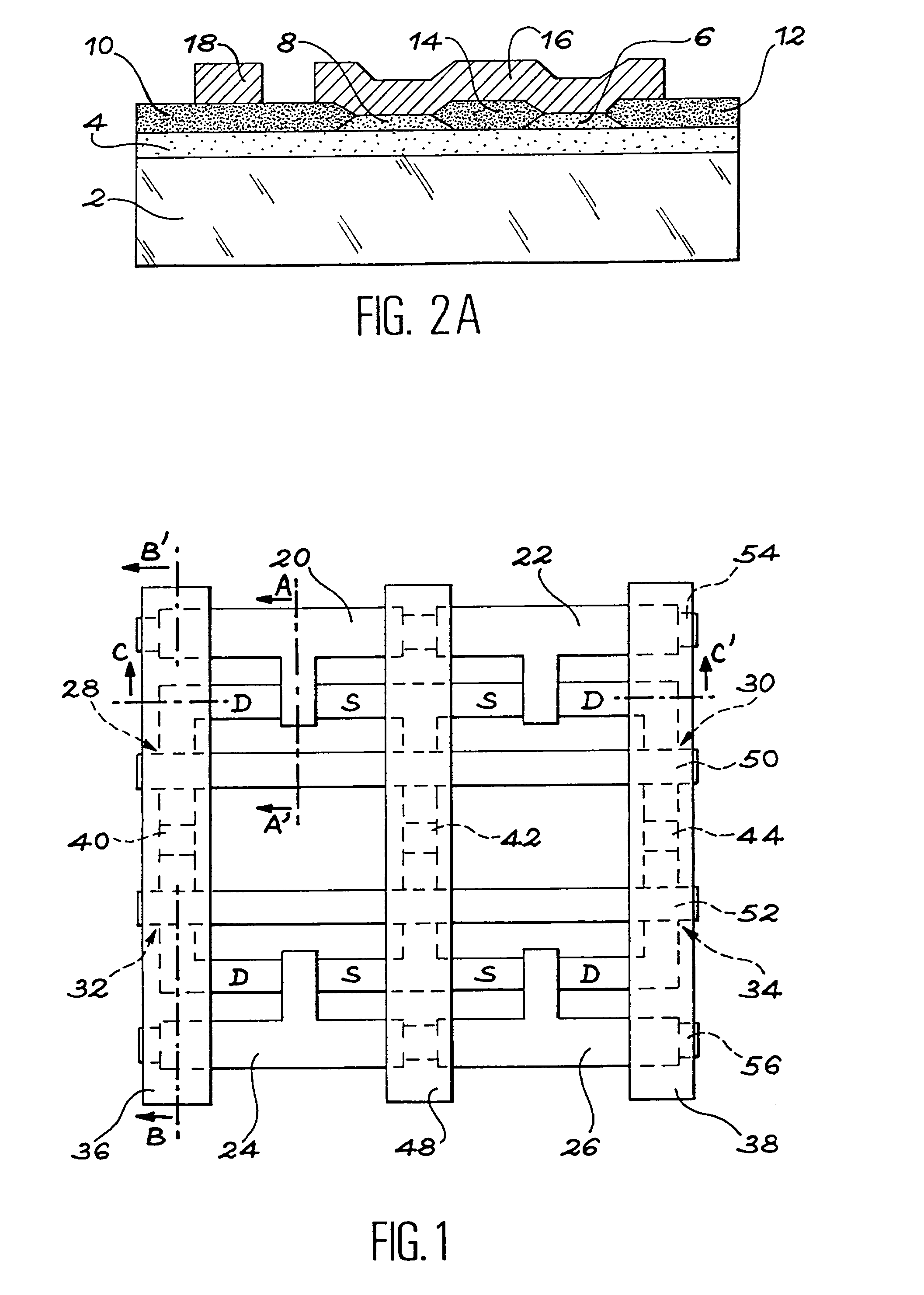
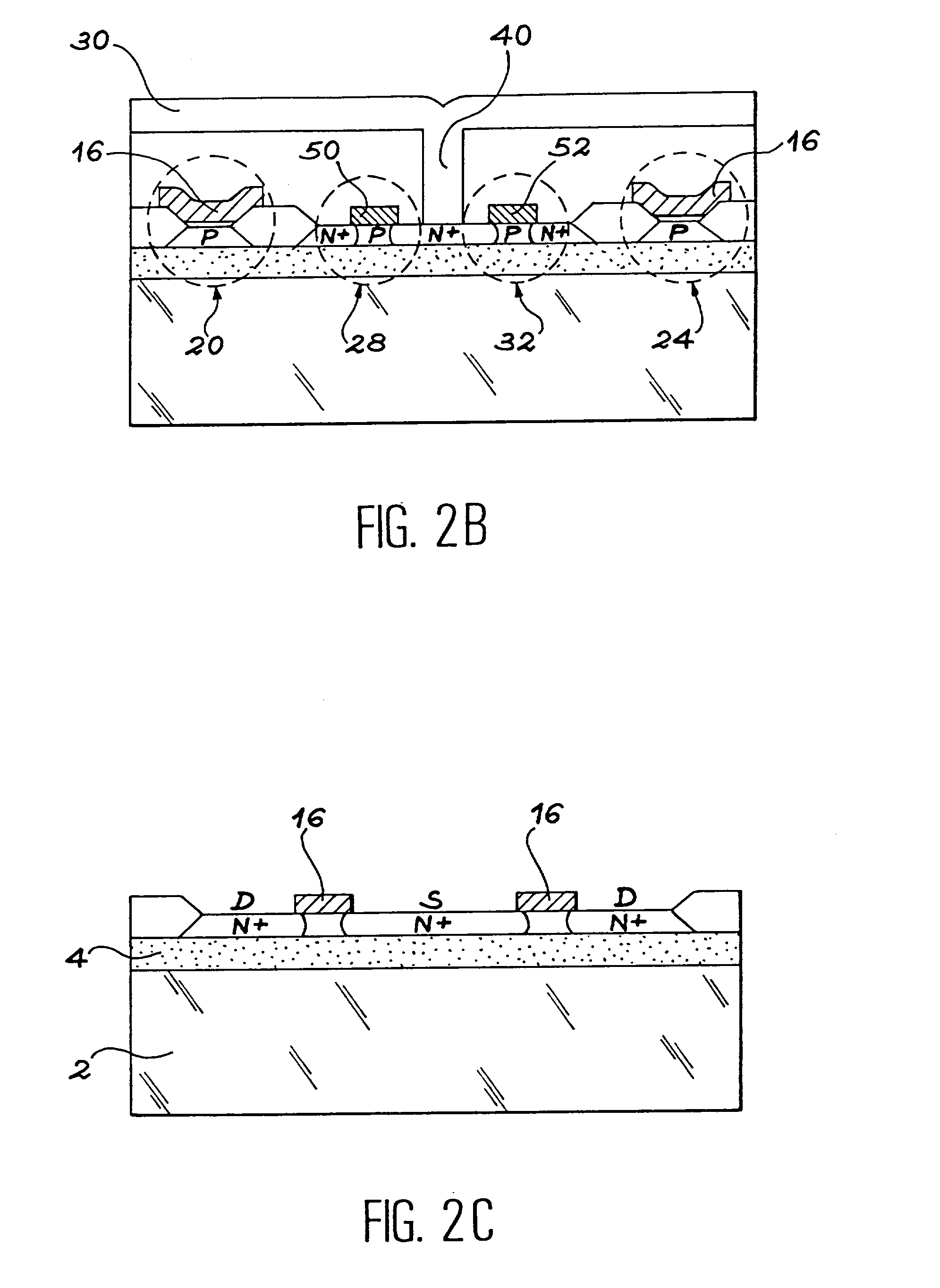
[0008] More specifically, the invention relates to an electrically erasable, non-volatile memory device, having a memory cell of the floating gate type, defined by a source zone, a drain zone, a channel zone and a control gate zone, the latter being separated from the channel zone by an insulation zone, said five zones being implemented in a semiconductor film formed on an insulating layer, said memory cell being laterally insulated by one or more insulation zones in contact with the insulating layer.

[0009] The invention also relates to an electrically erasable, non-volatile memory device having, in a semiconductor film separated by an insulating layer from a substrate, at least one memory ce...


PUM


Abstract

The invention relates to an electrically erasable, non-volatile memory device, having a memory cell of the floating gate type (16), defined by a source zone, a drain zone, a channel zone (8) and a control gate zone (6), the latter being separated from the channel zone by an insulation zone (14), said five zones being implemented in a semiconductor film formed on an insulating layer (4), said memory cell being laterally insulated by one or more insulation zones (10, 12) in contact with the insulating layer.

Description

TECHNICAL FIELD AND PRIOR ART[0001] The present invention relates to a bit by bit selectively and electrically erasable, programmable, non-volatile memory device (EEPROM). The use of a standard CMOS / SOI technology, i.e. without any specific technological stage, makes it possible to envisage the integration of such EEPROM memory cells into CMOS logic circuits without any modification of the production technology.[0002] Electrically erasable, programmable, non-volatile memories have existed since the mid-1970's (FLOTOX cell invented by INTEL). They are characterized by a manufacturing process having two polycrystalline silicon levels (floating gate and control gate), generally high erasing and programming voltagegs (>15 V) and a complex memory cell with an access transistor, a double gate transistor and an erasing zone with a very small gate oxide thickness (tunnel oxide).[0003] For reasons of technological complexity and the large surface area of the memory cell, this type of prod...

Claims


Application Information

Patent Timeline
Patent Type & Authority Applications(United States)
IPC IPC(8): H01L21/8247H01L21/84H01L27/12H10B69/00
CPCH01L21/84H01L27/115H01L27/1203H01L27/11558H01L27/11521H10B41/60H10B69/00H10B41/30
Inventor HARTMANN, JOELBELLEVILLE, MARC
Owner COMMISSARIAT A LENERGIE ATOMIQUE ET AUX ENERGIES ALTERNATIVES
Learn More