Liquid crystal display device

a display device and liquid crystal technology, applied in static indicating devices, cathode-ray tube indicators, instruments, etc., can solve problems such as overshooting, unsatisfactory visibility of display, and possibility of undershooting

Inactive Publication Date: 2002-04-25
TRIVALE TECH
View PDF5 Cites 32 Cited by
  • Summary
  • Abstract
  • Description
  • Claims
  • Application Information

AI Technical Summary

Problems solved by technology

However, when this technique is applied to a liquid crystal panel with a comparably high response speed of the liquid crystal element as some 10 ms, such as the recent TFT-LCD using a thin film transistor, for example, when the electrical signal waveform 101 is switched from the low voltage level into the high voltage as shown in FIG. 9(a), there is a possibility that an overshooting occurs in the optical response waveform 102, as shown in FIG. 9(b), which is not desirable in terms of visibility of the display.
On the other hand, when the voltage level is switched from the high level to the low level, there is a possibility that an undershooting occurs.
Furthermore, when the signal level after switching the display reaches the highest level, the compensation signal with a level higher than this highest level cannot be generated, which leads to a problem that disables improvement of the response speed.

Method used


Image

  • Liquid crystal display device
  • Liquid crystal display device
  • Liquid crystal display device

Examples


embodiment 2

[0038] The Embodiment 2

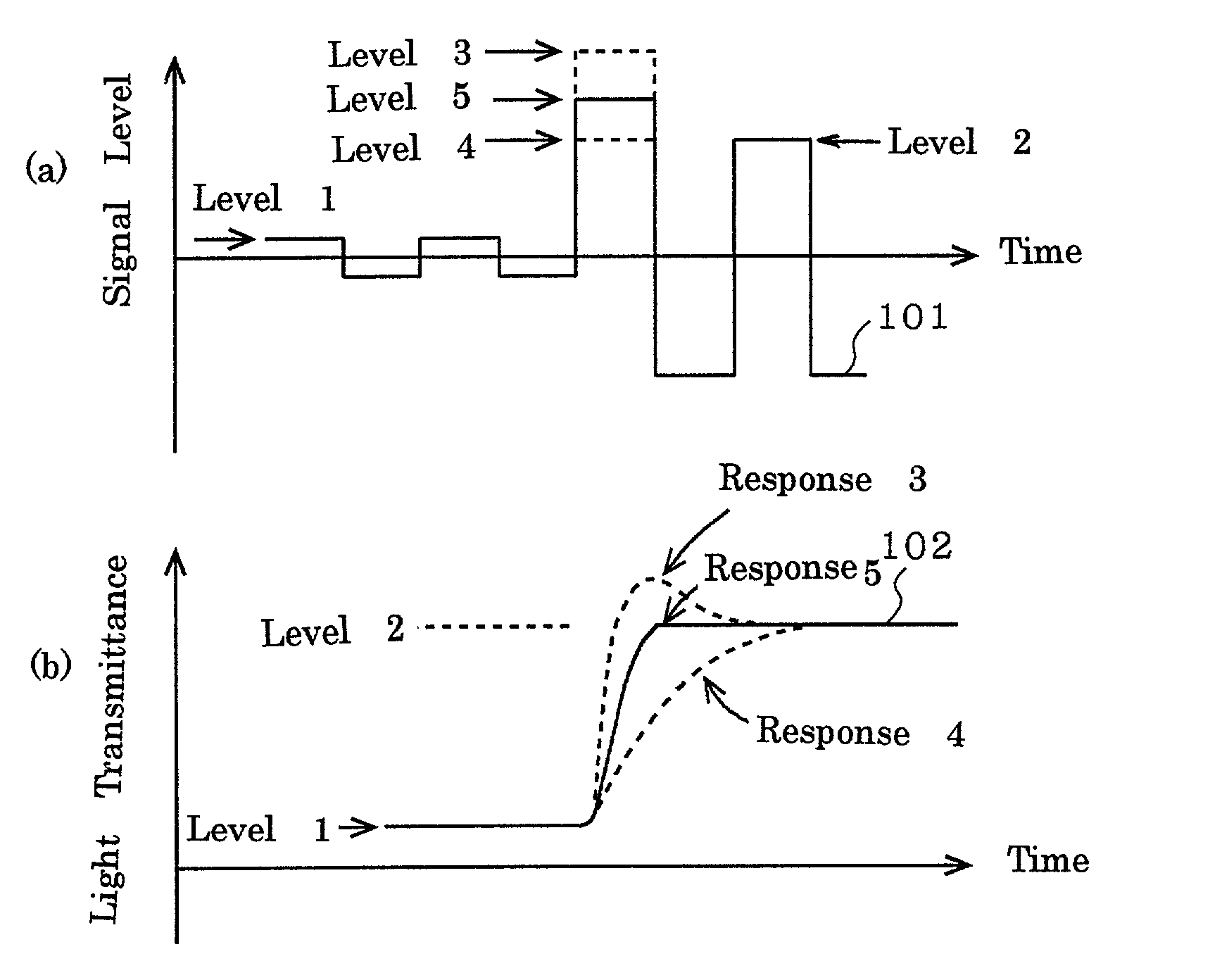
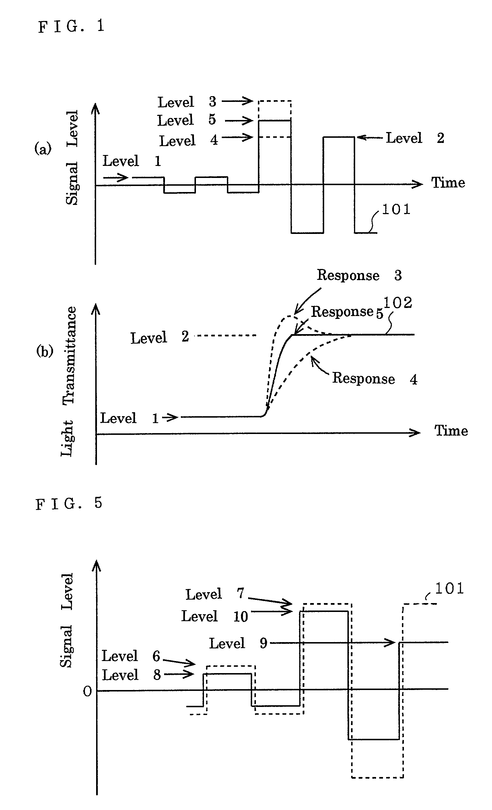
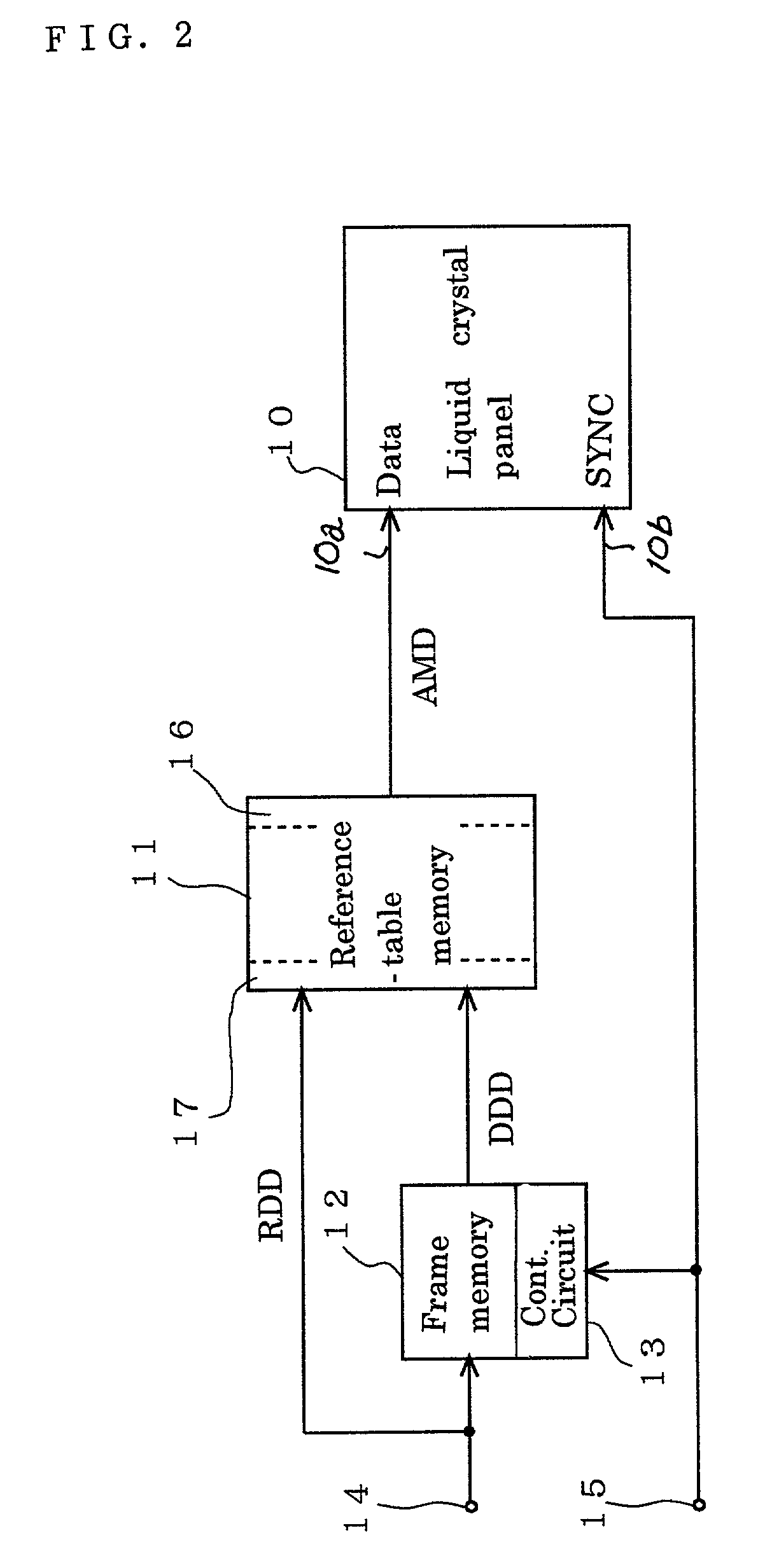
[0039] Next, a concrete method of generating the compensation signal while always compressing the original signal will be described. In a liquid crystal panel that can provide displays of 8 bits, namely, 256 levels, a data compression standard of 200 / 256, for example, is set. If the signal level before the one display period (the delayed display data DDD) is equal to the current signal level (the current display data RDD), the diagonal value on the table in FIG. 3, for example, will be selected as the compensation data AMD, but in the Embodiment 1, the data of the original signal level was written here on the diagonal as it was. In this Embodiment 2, as shown in FIG. 4, as a data when the signal level before the one display period (the delayed display data DDD) is equal to the current signal level (the current display data RDD), the data in which the original data is compressed to 200 / 256 (compression depth is 256 minus 200) is provided in advance on the diago...

embodiment 3

[0041] The Embodiment 3

[0042] In the Embodiment 2, since the signal level supplied to the liquid crystal panel is compressed, the luminance will be lowered on the display. Accordingly, there is a possibility that the difference of the luminance brings about a sense of incongruity, when the liquid crystal panel is switched from the regular drive to the drive with a compression. In that case, as shown in FIG. 6, the signal compression is carried out during driving the liquid crystal panel, in a manner that the switching of the regular drive and the drive with a compression is interlocked with the luminance switching of the backlighting of the liquid crystal panel. And in this case, the luminance of the backlighting is raised to compensate the lowering of the luminance due to the lowering of the signal level, thereby achieving the display state with a desirable luminance.

[0043] In FIG. 6, S1 and S2 signify switches that interlock each other. The switch S1 has a regular drive contact a ...


PUM

PropertyMeasurementUnit
switching timeaaaaaaaaaa
light transmittanceaaaaaaaaaa

Abstract

The invention relates to a liquid crystal display device, comprising a memory that delays a current display data supplied to a liquid crystal panel by one display period, and a reference table memory that holds a reference data containing multiple reference values determined by the current display data and a delayed displayed data. Here, the reference table memory has a compensation signal data written in advance, which substantially completes an optical response of the liquid crystal panel within the one display period. The liquid crystal display device supplies the inputted display data after having been converted always into a compensated signal level data to the liquid crystal panel, thus achieving a high-speed response that is completed within the one display period.

Description

[0001] 1. Field of the Invention[0002] The present invention relates to a liquid crystal display device using a liquid crystal panel.[0003] 2. Related Art[0004] A liquid crystal panel switches display levels of a picture by switching electrical signals from outside. The liquid crystal panel usually receives display data from outside, converts the display data into electrical signal waveforms of predetermined voltage levels, and applies the waveforms to the liquid crystal elements to thereby display a picture. The switching time of the display levels by the liquid crystal panel is some 10 ms in general.[0005] FIG. 7 illustrates an example of response waveform when an electrical signal is applied to one liquid crystal element. In FIG. 7(a), an electrical signal waveform 101 illustrates a voltage applied to the liquid crystal element. The horizontal axis represents the time and the vertical axis represents the signal level. T1 represents a period of time during which a low signal level...

Claims


Application Information

Patent Timeline
Patent Type & Authority Applications(United States)
IPC IPC(8): G02F1/133G09G3/20G09G3/34G09G3/36G09G5/36
CPCG09G3/3406G09G3/3685G09G5/36G09G2340/16G09G2320/0285G09G2320/0633G09G2320/0646G09G2320/0252G09G3/36
Inventor MIYAKE, SHIRO
Owner TRIVALE TECH
Why Eureka
Try Eureka