Electric terminal for an electronic device

a technology of electronic devices and terminals, which is applied in the direction of sustainable manufacturing/processing, electrical apparatus casings/cabinets/drawers, and final product manufacturing, etc., can solve the problems of increasing the cost of electronic devices, and reducing the service life of electronic devices

Inactive Publication Date: 2002-06-06
RENESAS ELECTRONICS CORP
View PDF0 Cites 8 Cited by
  • Summary
  • Abstract
  • Description
  • Claims
  • Application Information

AI Technical Summary

Problems solved by technology

The is a problem in the basic structure of the flip-chip bonding structure of FIG. 1A that the under-filling step increases the fabrication steps and thus raises the cost of the electronic device.
In addition, the smaller pitch of the arrangement for the external terminals of the up-to-date electronic device due to the higher integration of the semiconductor devices renders the under-filling step itself difficult.
It is difficult to use the interposer substrate 35, however, for an electronic device having higher-density terminals because of the difficulty in arranging a large number of interconnecting wires with a higher density.
In addition, the thermal expansion of material used for the interposer sheet may damage the bonding structure to cause a crack 38 in the solder ball, as shown in FIG. 2B.
It is difficult, however, to design the diameter and the height of the conductive post 36 because a trade-off resides between the handling or testing of the electronic device and the reliability for the bonding structure of the electronic device.
This lowers the product yield of the electronic devices having such wires 37 irrespective of employing a BGA structure for the electric terminals.

Method used


Image

  • Electric terminal for an electronic device
  • Electric terminal for an electronic device
  • Electric terminal for an electronic device

Examples


Embodiment Construction

[0026] Now, the present invention is more specifically described with reference to accompanying drawings.

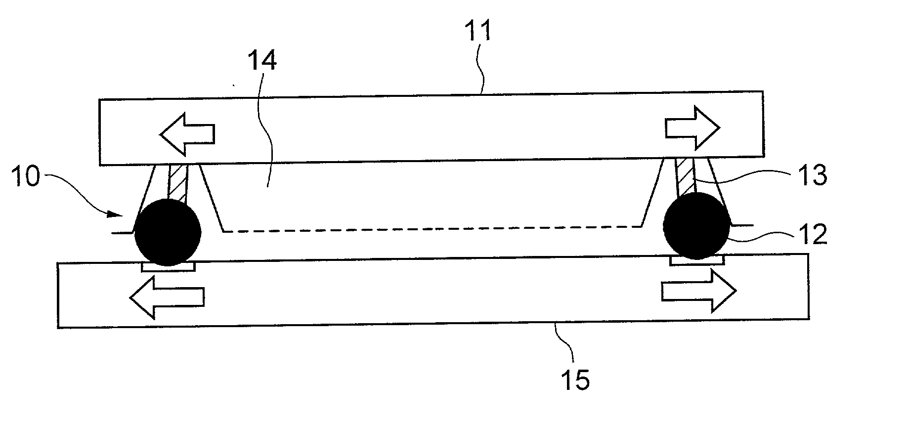
[0027] Referring to FIG. 3, an electric terminal, generally designated by numeral 10, according to an embodiment of the present invention is formed on an electronic device 11 such as an LSI. The electric terminal 10 includes a solder ball or external electrode 12, an elongate lead member 13 for electrically connecting the solder ball 12 to a pad 16 of the electronic device 11, and a support member 14 for mechanically supporting the solder ball 12 on the surface of the electronic device 11.

[0028] The lead member 13 has a resilience and thus absorbs the thermal stress occurring during a heat cycle test due to a difference in the thermal expansion coefficient between the electronic device 11 and a printed circuit board (not shown) on which the solder ball 12 is to be mounted. The lead member 13 is preferably made of a conductive material such as a metallic wire, or may be made of an...


PUM


Abstract

An electric terminal of an electronic device includes an external electrode, a flexible lead member for connecting the external electrode to a pad of the electronic device, and a support member for surrounding the lead member and mechanically supporting the external electrode when the lead member is deformed by a heat stress applied to the external electrode. By separating the electric connection function from the supporting function in the electric terminal, a reliable connection can be achieved after a heat cycle test of the electronic device.

Description

[0001] (a) Field of the Invention[0002] The present invention relates to an electric terminal for an electronic device and, more particularly, to the structure of an electric terminal for use in an electronic device and having a higher connection reliability. The present invention also relates to a method for forming such an electric terminal.[0003] (b) Description of the Related Art[0004] The reliability of an electronic device often depends on the connection reliability of the electric terminals used in the electronic devices. FIGS. 1A to 1D show conventional electric terminals used in semiconductor devices, which are to be mounted on respective printed circuit boards (mounting board) by using a flip-chip bonding technique. FIGS. 2A to 2D corresponding to FIGS. 1A to 1D, respectively, show the electric terminals after the heat cycle tests thereof.[0005] FIG. 1A shows the basic structure of the flip-chip bonding terminal called C4 type, wherein an external electrode implemented by ...

Claims


Application Information

Patent Timeline
Patent Type & Authority Applications(United States)
IPC IPC(8): H01L21/60H01L23/498H05K3/34H05K13/04
CPCH01L23/49816H01L2224/16225H04W8/20H05K3/3426H05K3/3436H05K2201/0367H05K2201/09472H01L2224/10125H01L24/11H01L24/13H01L24/16H01L2224/10126H01L2224/13017H01L2224/13023H01L2224/13082H01L2224/131H01L2224/13147H01L2224/136H01L2224/16227H01L2224/81191H01L2924/01078H01L2924/00014H01L2924/014H01L24/05H01L2224/05001H01L2224/05022H01L2224/05568H01L2224/05573H01L2224/056H01L2924/12042H01L2924/181H01L2924/351Y02P70/50H01L2924/00H01L2224/05099
Inventor KURITA, YOICHIRO
Owner RENESAS ELECTRONICS CORP
Why Eureka
Try Eureka