Method for fabricating array substrate for X-ray detector
a technology of array substrates and detectors, which is applied in the field of thin film transistor array substrates, can solve the problems of difficult to detect the gas produced, time-consuming film processing procedures, and difficult to accurately control the etching process
- Summary
- Abstract
- Description
- Claims
- Application Information
AI Technical Summary
Problems solved by technology
Method used
Image
Examples
first embodiment
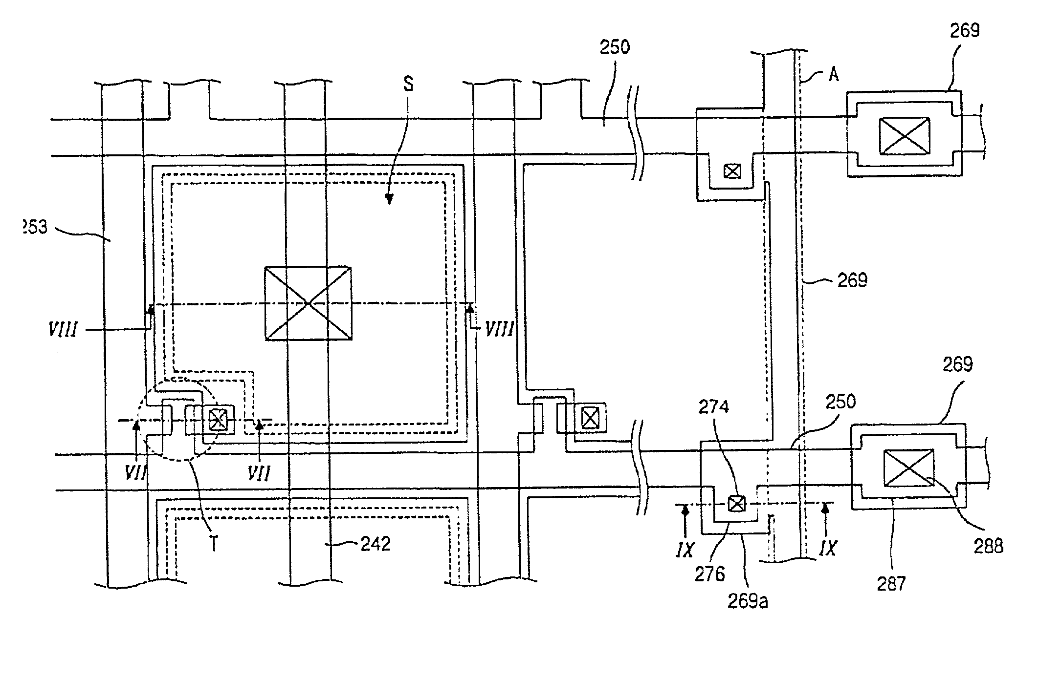
[0061] As described above, since the present invention employs the etching stopper on the first insulation layer, the etching ratio of the protection layer and the second insulation layer, which are stacked over the drain electrode and over the capacitor electrode, is controlled. Thus, over-etch caused by a difference in the number of etching layers is prevented. The EPD can also be employed.
second embodiment
[0062] Moreover, since the gate line is electrically connected to the etching stopper through the gate line contact hole in the second embodiment, gate line open-circuits caused by static electricity during a dry etching process are prevented. Therefore, the manufacturing yield is raised, and the manufacturing defect caused in the array substrate is decreased. The EPD can also be employed.
PUM
 Abstract
Description
Claims
Application Information


