Method of fusion for heteroepitaxial layers and overgrowth thereon
- Summary
- Abstract
- Description
- Claims
- Application Information
AI Technical Summary
Problems solved by technology
Method used
Image
Examples
Embodiment Construction
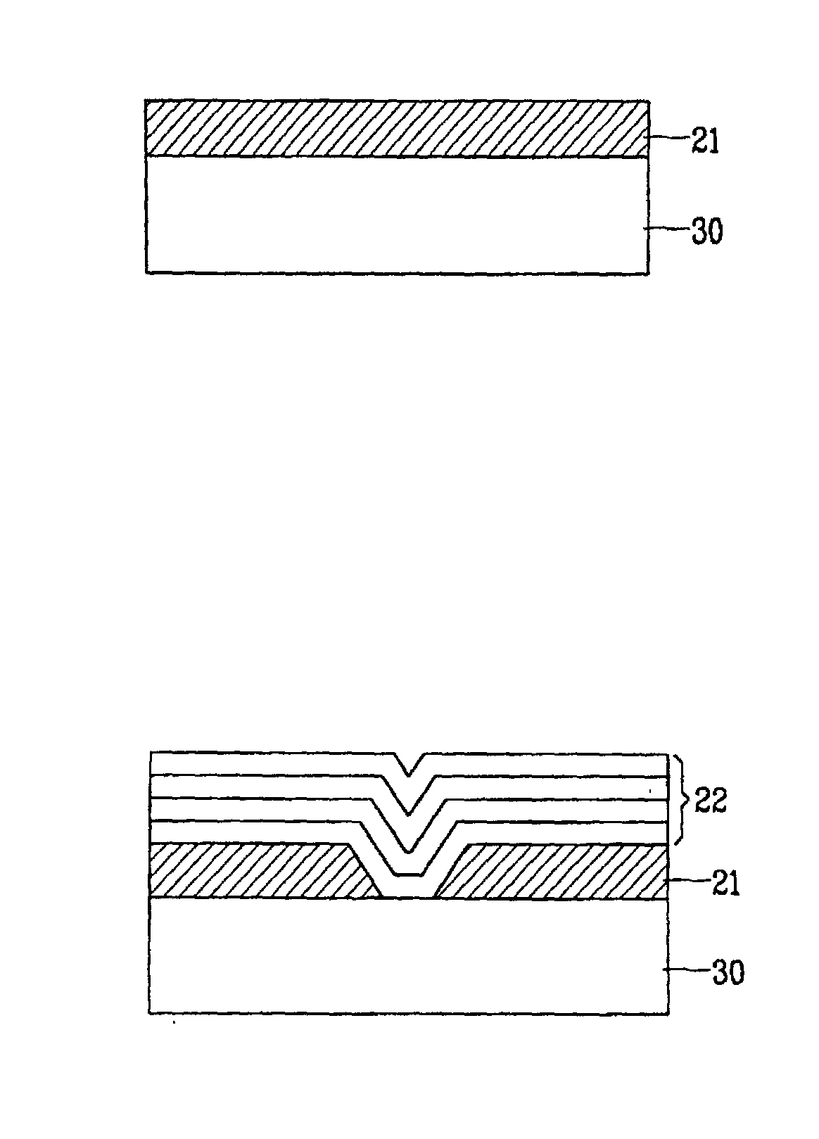
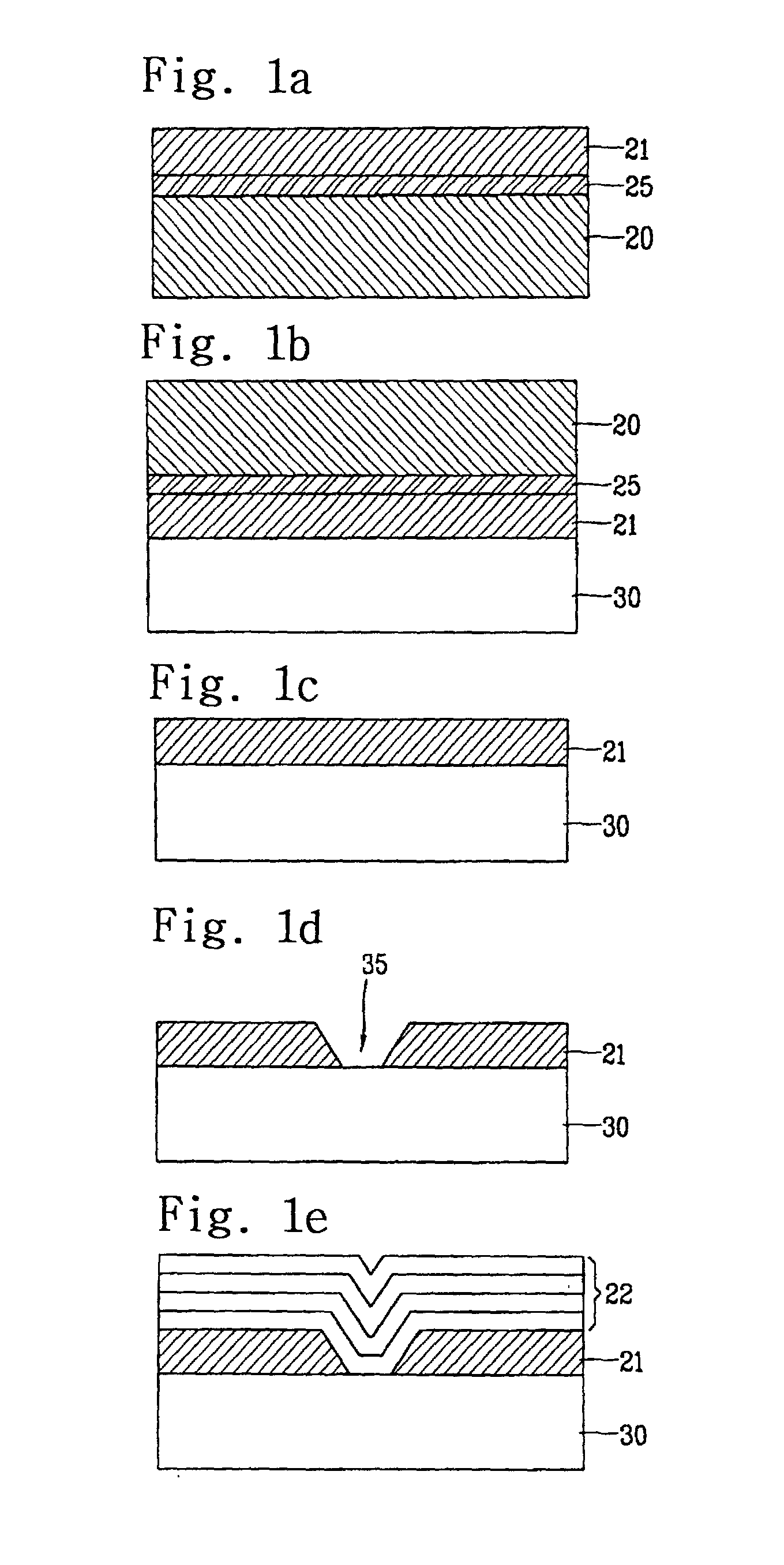
[0035] In the Example, the epitaxial growth of GaAs on InP and Si substrates having different lattice constants will be illustrated. FIGS. 1a to 1e are schematic diagrams for fabrication of heteroepitaxial growth according to the present invention.
[0036] An AlAs layer (25) was grown as a sacrificial layer on the GaAs substrate (25) to 500 .ANG.-5000 .ANG. at 750.degree. C. by the conventional APMOCVD(atmospheric pressure metalorganic chemical vapor deposition) technique. A GaAs epilayer (21) was then grown as a fusion layer to about 1500 .ANG. thickness (see FIG. 1a).
[0037] Since a large difference in the lattice constant between the first semiconductor substrate and the sacrificial layer causes a lattice relaxation to form line defects, etc., a material in which the lattice constant difference with the first semiconductor is 1% or less is preferably selected for the sacrificial layer. Further, the thickness of the sacrificial layer must be selected from the range in which a lattice...
PUM
 Abstract
Description
Claims
Application Information


