

Etch pattern definition using a CVD organic layer as an anti-reflection coating and hardmask
a technology of organic layer and anti-reflection coating, which is applied in the direction of basic electric elements, electrical apparatus, semiconductor devices, etc., can solve the problems of adversely affecting resolution and limited thickness of a given photoresist layer
- Summary
- Abstract
- Description
- Claims
- Application Information
AI Technical Summary
Benefits of technology
Problems solved by technology
Method used
Image

Examples
Embodiment Construction
[0027] As a preface to the detailed description, it should be noted that, all percentages (%) listed for gas constituents are % by volume, and all ratios listed for gas constituents are volume ratios.
[0028] The term "selectivity" is used to refer to a) a ratio of etch rates of two or more materials and b) a condition achieved during etch when etch rate of one material is increased in comparison with another material.
[0029] The present invention now will be described more fully hereinafter with reference to the accompanying drawings, in which preferred embodiments of the present invention are shown. This invention may, however, be embodied in different forms and should not be construed as limited to the embodiments set forth herein.
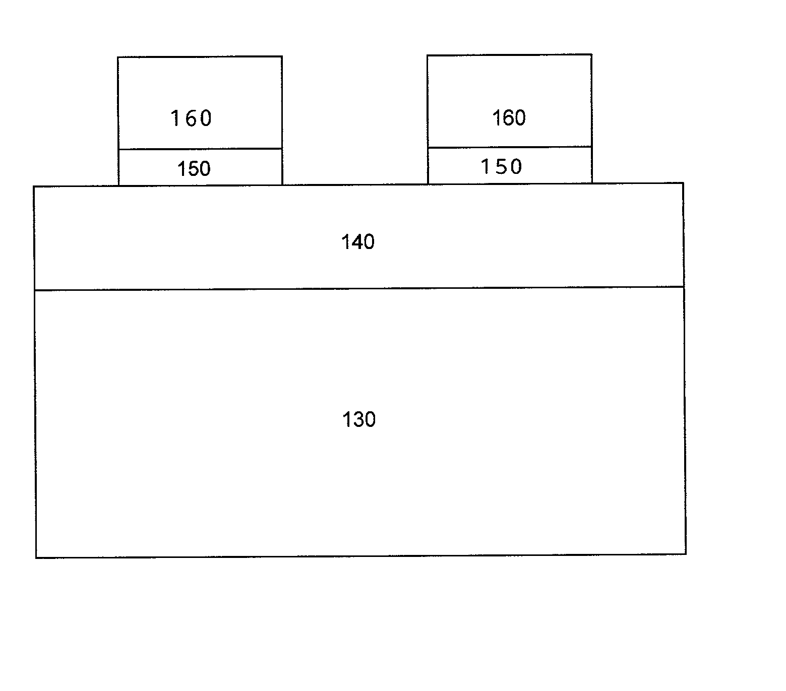
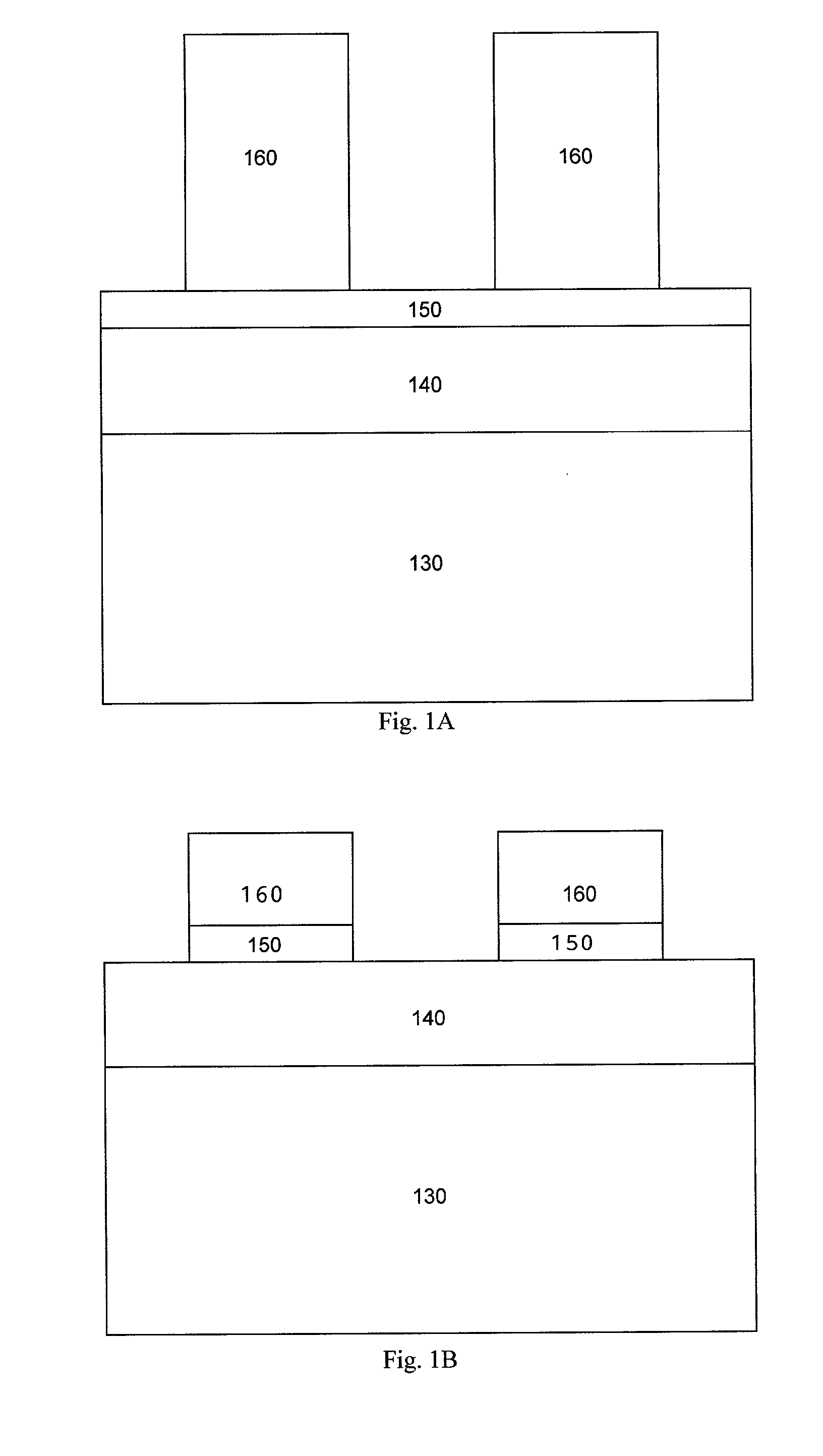
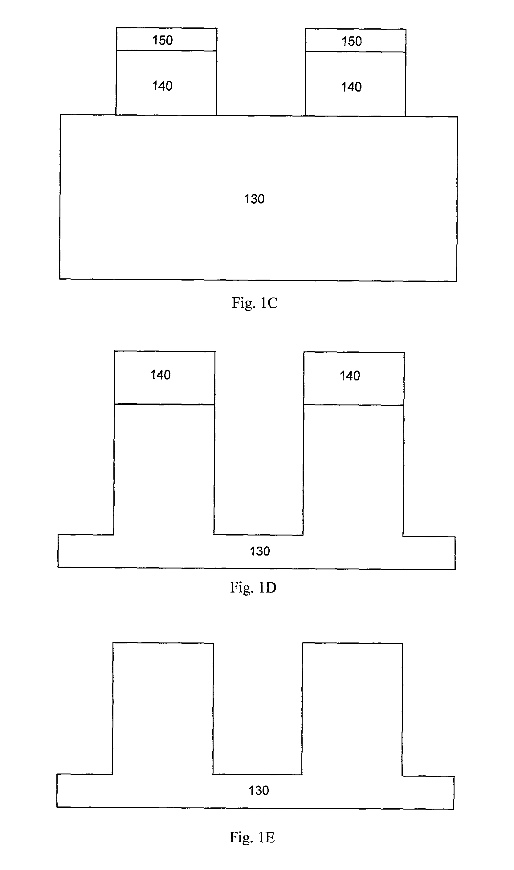
[0030] An embodiment of the present invention will now be described in connection with FIGS. 1A-1E. The multilayer structure illustrated in FIG. 1A includes a layer of material 130 to be etched, a chemical vapor deposited (CVD) organic layer 140, a dielect...
PUM
| Property | Measurement | Unit |
|---|---|---|
| thickness | aaaaa | aaaaa |
| refractive index | aaaaa | aaaaa |
| thicknesses | aaaaa | aaaaa |
Abstract
Description
Claims
Application Information