

Microwave-millimeter wave circuit apparatus and fabrication method thereof having a circulator or isolator
a technology of micro-millimeter wave circuit and circulator, which is applied in the direction of electrical equipment, resonators, and semiconductor devices, can solve the problems of mass production of equipment, rigidification of equipment, and difficulty in reducing the size and cost of equipment, etc., and achieves the reproducibility of apparatus performance. reproducibility, the effect of reducing the size of the equipmen
- Summary
- Abstract
- Description
- Claims
- Application Information
AI Technical Summary
Problems solved by technology
Method used
Image

Examples
first embodiment
[0030] [First Embodiment]
[0031] FIGS. 2A and 2B are a plan view and a sectional view showing an example of the structure of a microwave-millimeter wave circuit apparatus according to a first embodiment of the present invention.
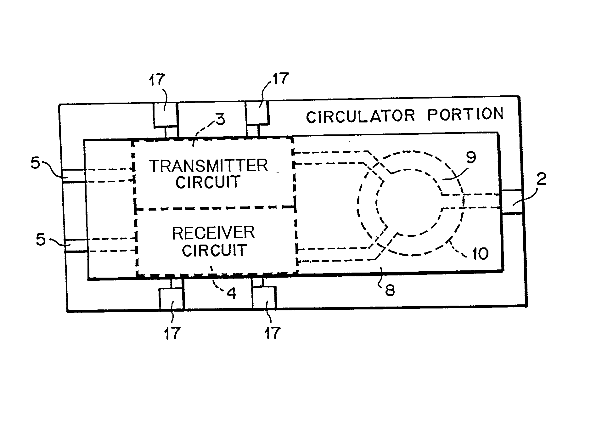
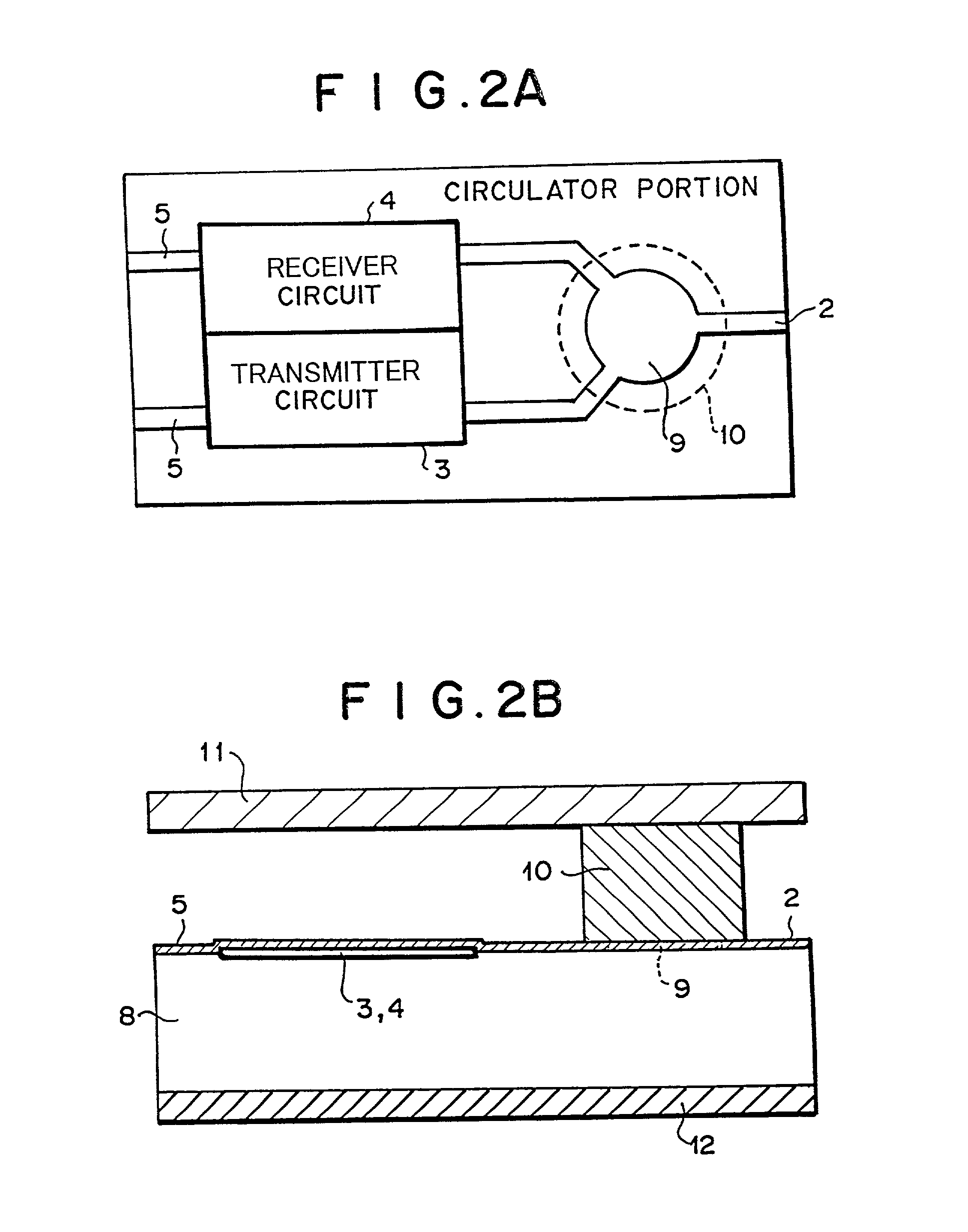
[0032] Referring to FIGS. 2A and 2B, a transmitter circuit 3 and a receiver circuit 4 are formed on an MMIC substrate 8. In addition, a pattern 9 for a circulator is formed on the MMIC substrate 8. One surface of ferrite 10 contacts the pattern 9. A grounding metal layer or a metal cover 11 is disposed on the other surface of the ferrite. A grounding metal layer 12 is formed on the other surface of the MMIC substrate 8. In the first embodiment, lines of the circulator are of tri-plate type of which a signal line is formed between the ferrite and the MMIC substrate 8 having a grounding metal layer 12 and between the metal cover 11 and the ferrite. The transmitter circuit 3 has a power amplifying circuit, a radio frequency converter, and a modulating circuit. Th...
second embodiment
[0039] [Second Embodiment]
[0040] FIGS. 6A and 6B are a plan view and a sectional view showing a first example of the structure of a microwave-millimeter wave circuit apparatus according to a second embodiment of the present invention. The microwave-millimeter wave circuit apparatus shown in FIGS. 6A and 6B is composed of an MMIC substrate 8 and a dielectric substrate 15. A transmitter circuit 3, a receiver circuit 4, and a pattern 9 for a circulator are formed on the MMIC substrate 8. Ferrite 10 for a circulator is embedded in the dielectric substrate 15. The dielectric substrate 15 is for example a glass ceramic substrate. The MMIC substrate 8 and the dielectric substrate 15 are oppositely aligned. The dielectric substrate 15 has an RF signal terminal 2, an IF signal terminal 5, and a bias terminal 17. The transmitter circuit 3, the receiver circuit 4, and the pattern 9 for the circulator formed on the MMIC substrate 8 are connected with bumps 16. The ferrite 10 and the pattern 9 a...
third embodiment
[0044] [Third Embodiment]
[0045] FIGS. 10A and 10B are a plan view and a sectional view showing an example of the structure of a microwave-millimeter wave circuit apparatus according to a third embodiment of the present invention. In the structure shown in FIGS. 10A and 10B, only a transmitter circuit and a receiver circuit are formed on an MMIC substrate 8. Patterns 2, 5, and 9 for a circulator and so forth and a bias terminal 17 are formed on a dielectric substrate 15. Ferrite 10 is embedded in the dielectric substrate 15. The MMIC substrate 8 and the dielectric substrate 15 are connected by flip-chip method. In the structure shown in FIGS. 10A and 10B, since the patterns 2, 5, and 9 for the circulator and so forth and the bias terminal 17 are formed on the dielectric substrate 15, the MMIC substrate 8 can be compactly structured.
[0046] FIGS. 11A and 11B are a plan view and a sectional view showing another example of the structure of the microwave-millimeter wave circuit apparatus ...
PUM
 Abstract
Description
Claims
Application Information