Optical mode expander

a technology of optical expansion and optical mode, applied in the direction of lasers, instruments, electrical equipment, etc., can solve the problems of inp based devices, however, and a number of limitations

Inactive Publication Date: 2002-07-18
KAMELIAN A BODY
View PDF0 Cites 0 Cited by
  • Summary
  • Abstract
  • Description
  • Claims
  • Application Information

AI Technical Summary

Problems solved by technology

InP based devices, however, have a number of limitations.

Method used


Image

  • Optical mode expander
  • Optical mode expander
  • Optical mode expander

Examples


Embodiment Construction

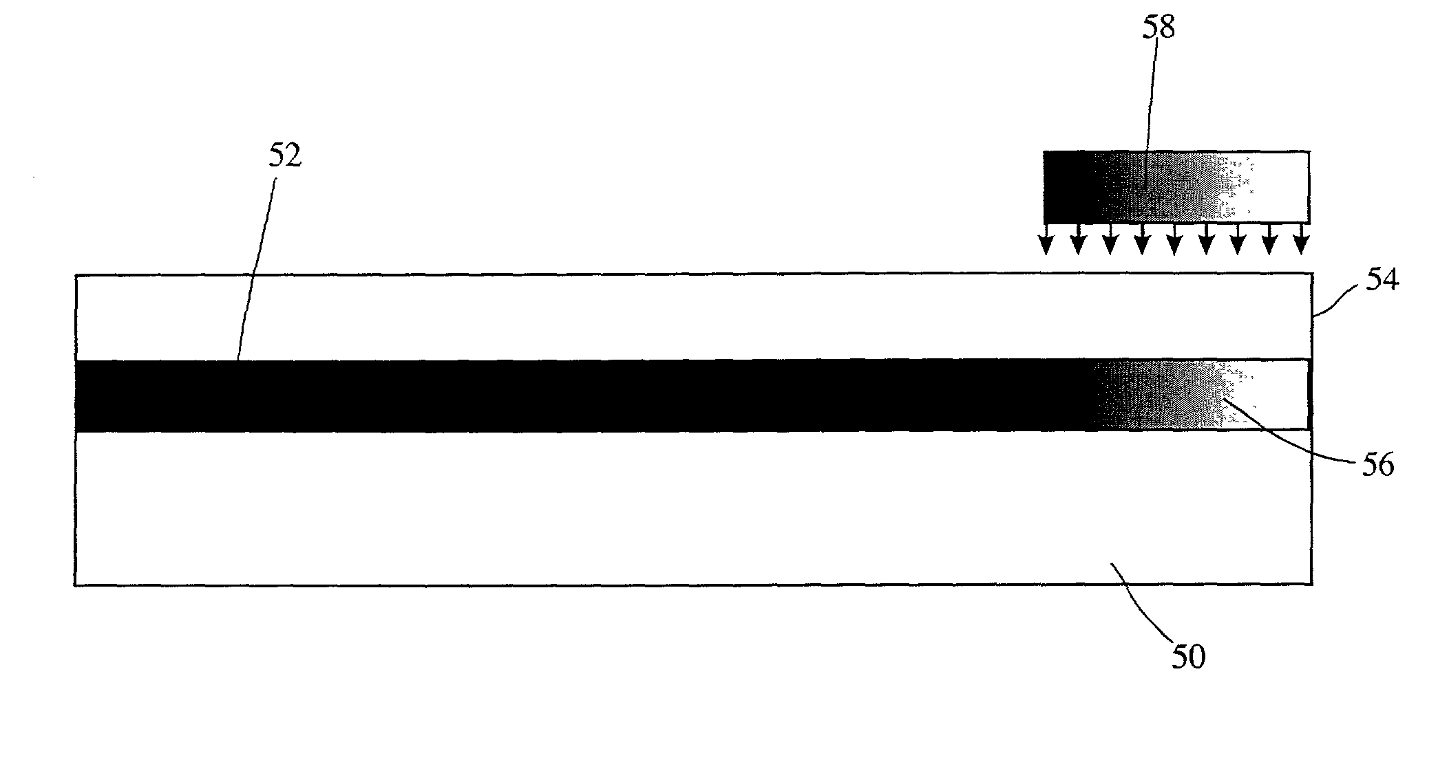
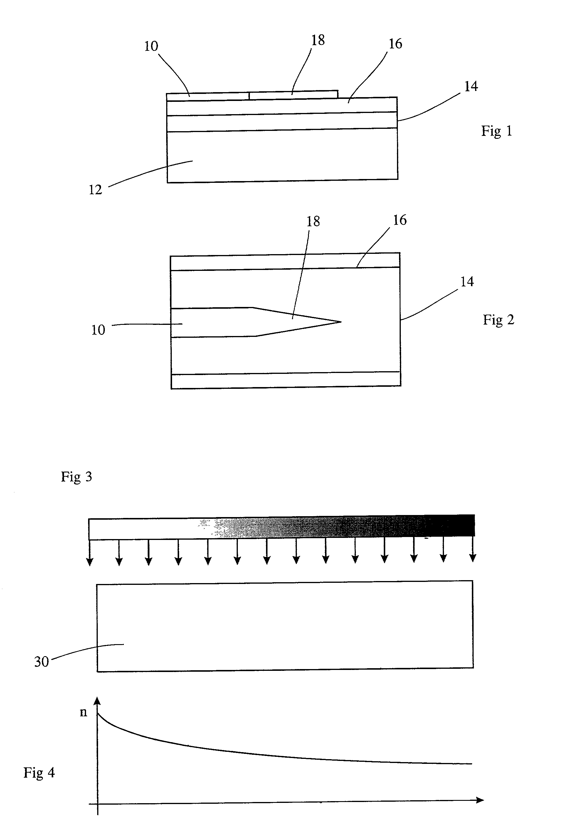
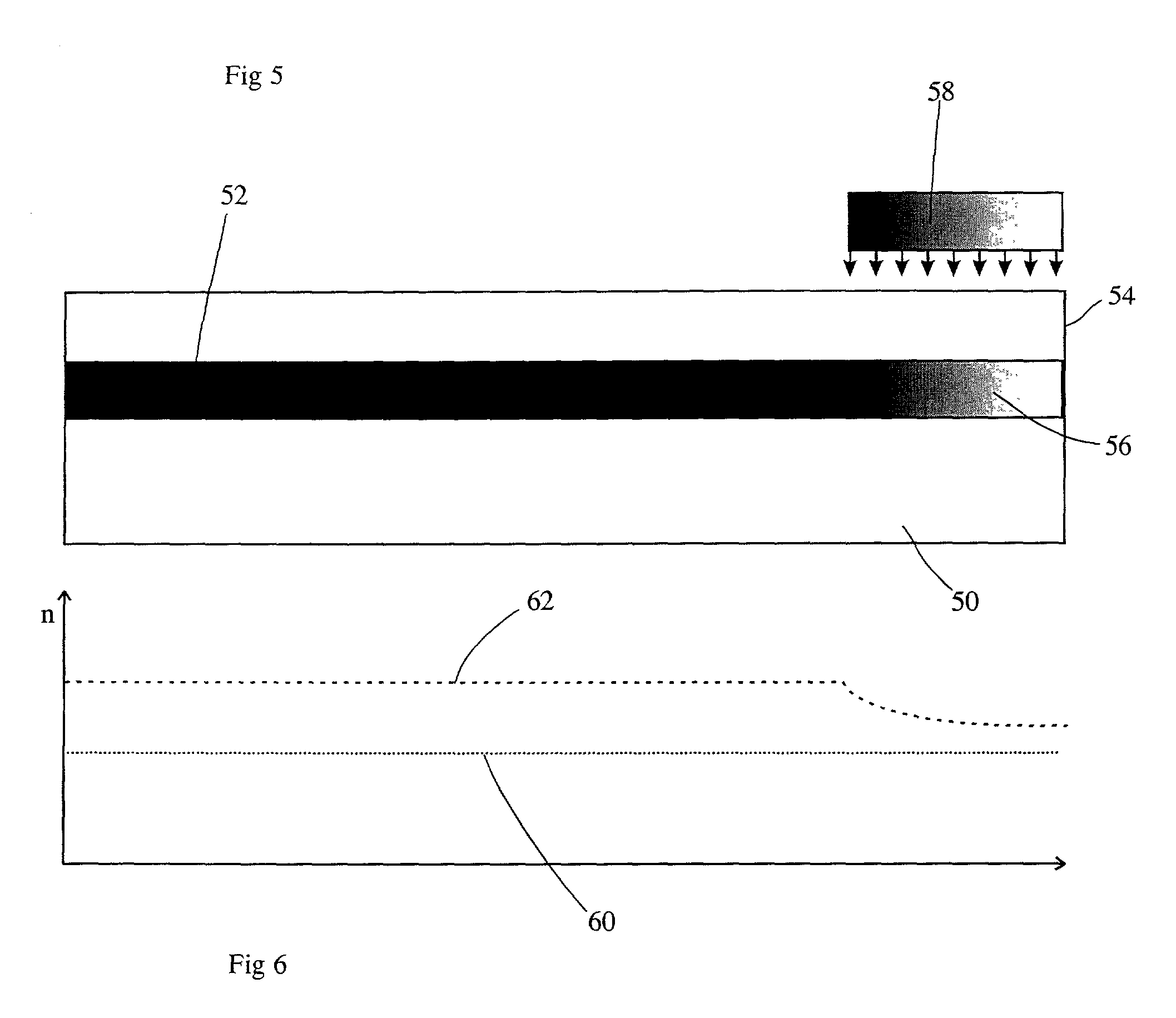
[0020] One of the most important characteristics of any active device is it's suitability for packaging since most of the cost in manufacture is incurred during this process. Due to the tightly guided modes in (In, Ga)(As, P) devices and the dilute mode of the optical fibre or passive waveguides, the devices have to be actively packaged to very tight alignment tolerances, typically using lenses. One way around this is to use mode expanders at the facet of the device where the optical mode is expanded to the size required. This then allows passive alignment of the devices to optical fibre or waveguides. Usually these mode expanders are formed by introducing a taper to the active region to direct the optical mode towards an underlying passive waveguide.

[0021] FIG. 1 shows a typical mode expander. A main waveguide 10 defined on the epi layer 12 approaches the facet 14. A wider waveguide 16 is defined beneath the main waveguide 10. Near the facet 14, the main waveguide narrows to a tape...


PUM


Abstract

A semiconductor optical amplifier comprising an active gain region of the (In, Ga)(As, N) system is proposed, together with the use of (Ga, In)(As, N) as the base material for the fabrication of an SOA, and a semiconductor optical amplifier comprising (Ga, In)(As, N) as the base material. The N content of the (In, Ga)(As, N) can be varied along a dimension of the active region in the direction of propagation of light signals therein, to create a varying bandgap such as for mode expanders. The active region can be supplied by a source of electrical bias which is applied in segments along the dimension of the active region, the segments being capable of independent variation. This should allow channel equalisation of WDM signals to be performed dynamically. This scheme could also be used to equalise device parameters such as differential gain, saturation output power and linewidth enhancement factor across the amplification bandwidth.

Description

[0001] The present invention relates to semiconductor optical mode expanders. In particular, it proposes the use of the GaInNAs material system in this context. The invention flows from the discovery that the use of this material system should allow a number of novel devices to be fabricated which would not be feasible using the previous materials systems such as InP.BAKGROUND ART[0002] Mode expanders are used in optical devices where it is desired to expand the mode of light propagating along the length of an optoelectronic device. These expanders are applicable to optical fibres in particular where the mode of an optoelectronic device may be expanded to facilitate alignment of the two components. Mode expansion is particularly applicable to semiconductor optical amplifiers (SOAs). Presently mode expansion is achieved by introducing a parallel, wider waveguide, beneath the narrow waveguide which is tapered such that the optical mode is forced into the underlying waveguide thus incr...

Claims


Application Information

Patent Timeline
Patent Type & Authority Applications(United States)
IPC IPC(8): G02B6/12G02B6/122G02B6/30
CPCG02B6/1228G02B6/305G02B2006/12195
Inventor TOMBLING, CRAIGKEAN, ALISTAIR HENDERSONDAWSON, MARTIN DAVIDKELLY, ANTHONY EDWARD
Owner KAMELIAN A BODY
Why Eureka
Try Eureka