
Protective film separator in semiconductor wafer grinding process

a technology of protective film and semiconductor wafer, which is applied in the direction of grinding machines, manufacturing tools, lapping machines, etc., can solve the problems of adversely affecting the final yield of the final wafer, increasing the expense of raw materials, and severe stress on the wafer surfa

Inactive Publication Date: 2002-07-18
SAMSUNG ELECTRONICS CO LTD
View PDF0 Cites 29 Cited by
  • Summary
  • Abstract
  • Description
  • Claims
  • Application Information

AI Technical Summary

Benefits of technology

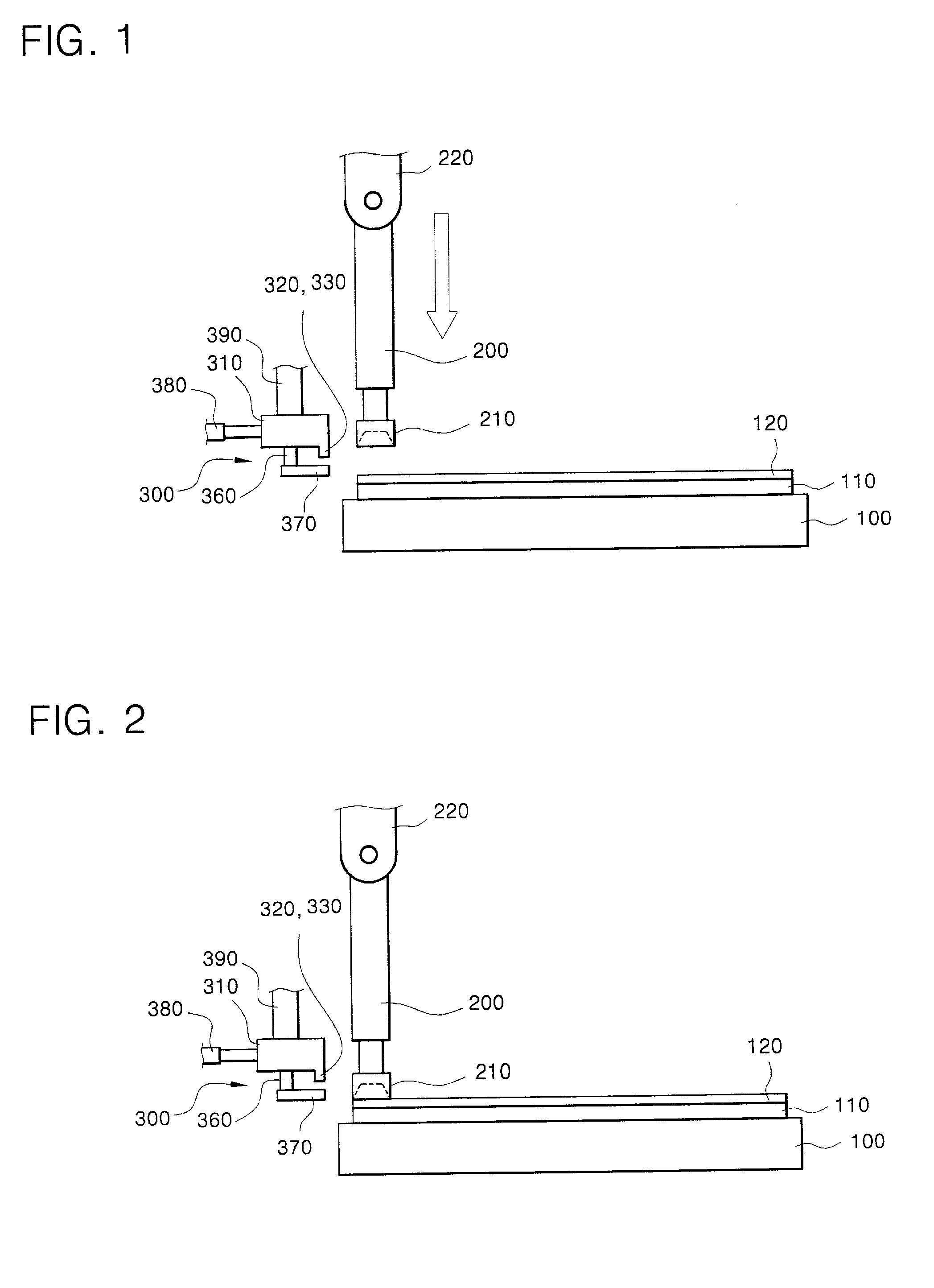
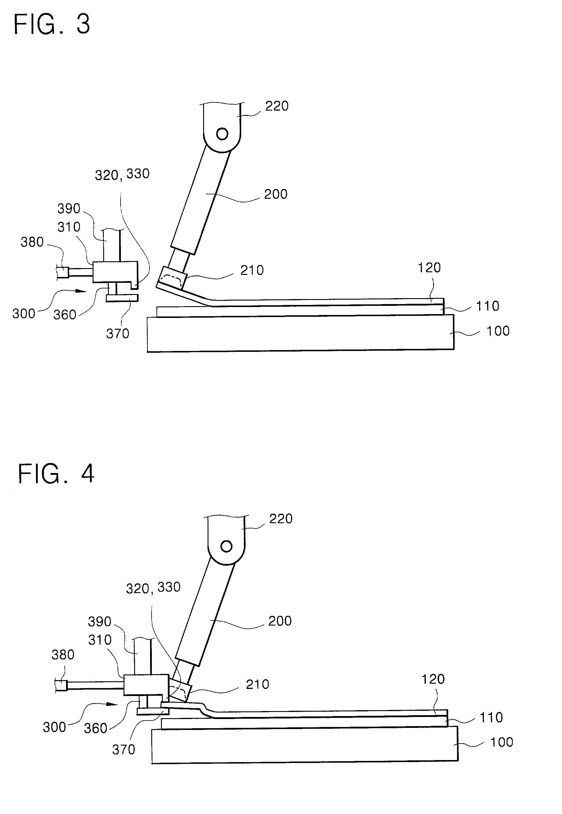
[0013] Another feature of an embodiment of the present invention provides a protective film separator that reduces an external force applied to a wafer, thereby preventing a patterned side of the wafer from obtaining impurities while the protective film is removed.

Problems solved by technology

The two conventional types of protective film separators continuously consume extra tape, i.e. the extra removing tape and the heat-activated adhesive tape, which causes a continuous increase in the expense of raw materials.
Additionally, either the roller or the heater for removing the protective film presses against the wafer thereby generating severe stress on the wafer surface.
Moreover, impurities or residue stained in the protective film can cause damage to the patterned wafer by virtue of the physical contact, which further adversely affects the final wafer yields.

Method used


Image

  • Protective film separator in semiconductor wafer grinding process
  • Protective film separator in semiconductor wafer grinding process
  • Protective film separator in semiconductor wafer grinding process

Examples


Embodiment Construction

[0028] Korean Patent Application No. 2001-2681, filed on Jan. 17, 2001, and entitled: "Protective Film Separator in Semiconductor Wafer Grinding Process", is incorporated by reference herein in its entirety.

[0029] The present invention now will be described more fully with reference to the accompanying drawings, in which preferred embodiments of the invention are shown. This invention may, however, be embodied in many different forms and should not be construed as being limited to the embodiments set forth herein; rather, these embodiments are provided so that this disclosure will be thorough and complete, and will fully convey the concept of the invention to those of ordinary skill in the art.

[0030] In general, a semiconductor process includes a single crystal silicon growing process, a device design process, a fabrication FAB process, an assembly process, and an inspection process. The single crystal silicon growing process produces a single crystal silicon ingot with a high purit...


PUM

PropertyMeasurementUnit
rotationaaaaaaaaaa
adsorptionaaaaaaaaaa
distanceaaaaaaaaaa

Abstract

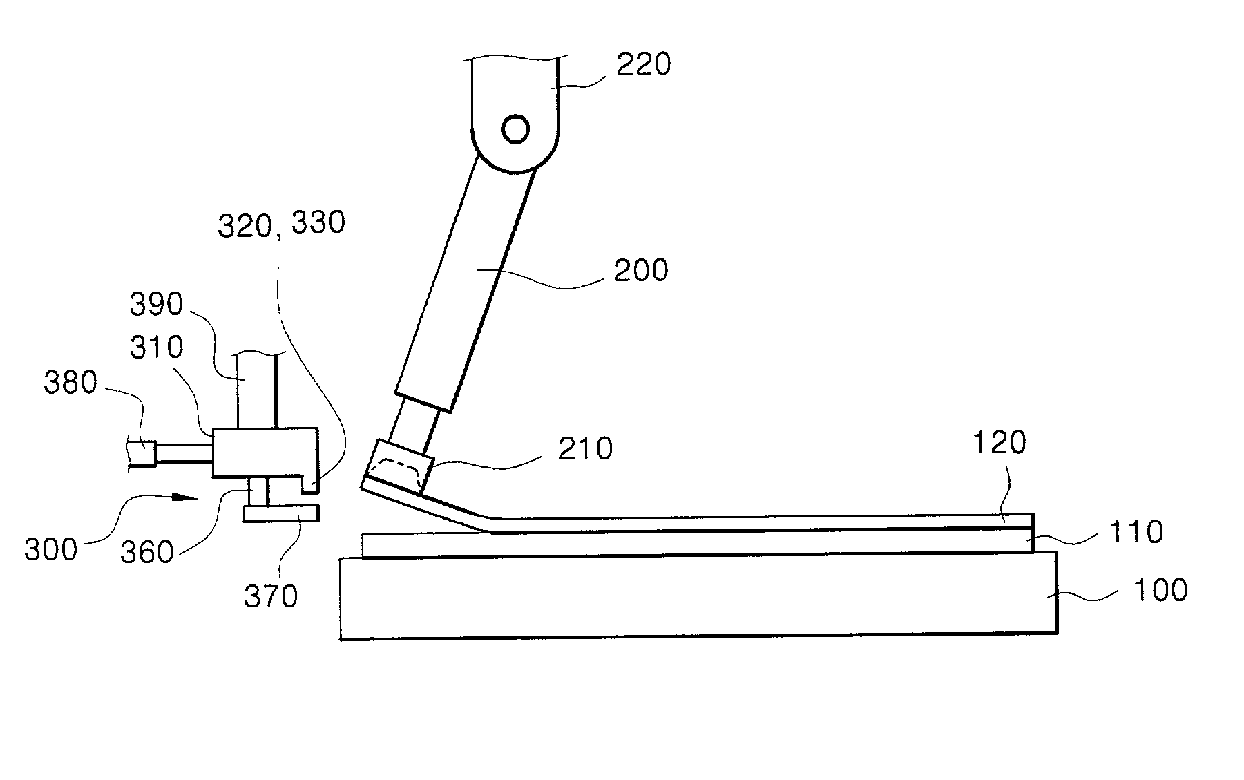
A protective film separator comprising an adsorption means and a peeling means for removing the protective film in a semiconductor wafer backside grinding process. The adsorption means uses a vacuum to separate a part of a protective film adhered to an electrical circuit patterned side of a wafer from the patterned side of the wafer. The peeling means presses each side of the part of the protective film separated from the wafer by the adsorption means, and separates unpeeled parts thereof from the patterned side of the wafer. The protective film separator of the present invention reduces costs and expenses for raw materials by eliminating the need for extra removing tape or heat-activated adhesive tape. The present invention may also improve semiconductor yields by reducing the external force applied to a wafer during removal of the protective film, thereby allowing better protection from impurities.

Description

[0001] 1. Field of the invention[0002] The present invention relates to a protective film separator in a semiconductor wafer grinding process, and more particularly, to a separator for removing a protective film affixed to an electric circuit patterned side of a wafer to protect the wafer in a semiconductor wafer grinding process.[0003] 2. Description of Related Art[0004] After completing an electric circuit patterning process to a side of a wafer in a semiconductor process, the other side of the wafer is generally ground in a wafer grinding process.[0005] The wafer grinding process polishes the backside of a wafer and removes a polysilicon layer or an oxide layer that is adhered to the backside of the wafer while the semiconductor process is performed. In addition, the wafer grinding process abrades the backside of a wafer making a thinner wafer, which results in simultaneous improvement in both electric and heat conductivity of a semiconductor device.[0006] Because such a wafer gr...

Claims


Application Information

Patent Timeline
Patent Type & Authority Applications(United States)
IPC IPC(8): H01L21/304B24B37/34B29C63/00
CPCB24B37/34B29C63/0013Y10S156/93Y10T156/1179H01L21/304
Inventor LIM, SANG SOON
Owner SAMSUNG ELECTRONICS CO LTD
Learn More