Eureka AIR delivers breakthrough ideas for toughest innovation challenges, trusted by R&D personnel around the world.

SOI semiconductor integrated circuit for eliminating floating body effects in SOI MOSFETs and method of fabricating the same

a technology of soi mosfet and semiconductor, which is applied in the field of semiconductor integrated circuit for eliminating floating body effects in soi mosfet and the method of fabricating the same, can solve the problems of lack of commercial success of soi integrated circuits

Inactive Publication Date: 2002-08-08
SAMSUNG ELECTRONICS CO LTD
View PDF0 Cites 16 Cited by
  • Summary
  • Abstract
  • Description
  • Claims
  • Application Information

AI Technical Summary

Problems solved by technology

SOI integrated circuits have suffered some lack of commercial success due to technical problems in material processing and device design.

Method used


Image

  • SOI semiconductor integrated circuit for eliminating floating body effects in SOI MOSFETs and method of fabricating the same
  • SOI semiconductor integrated circuit for eliminating floating body effects in SOI MOSFETs and method of fabricating the same
  • SOI semiconductor integrated circuit for eliminating floating body effects in SOI MOSFETs and method of fabricating the same

Examples


Embodiment Construction

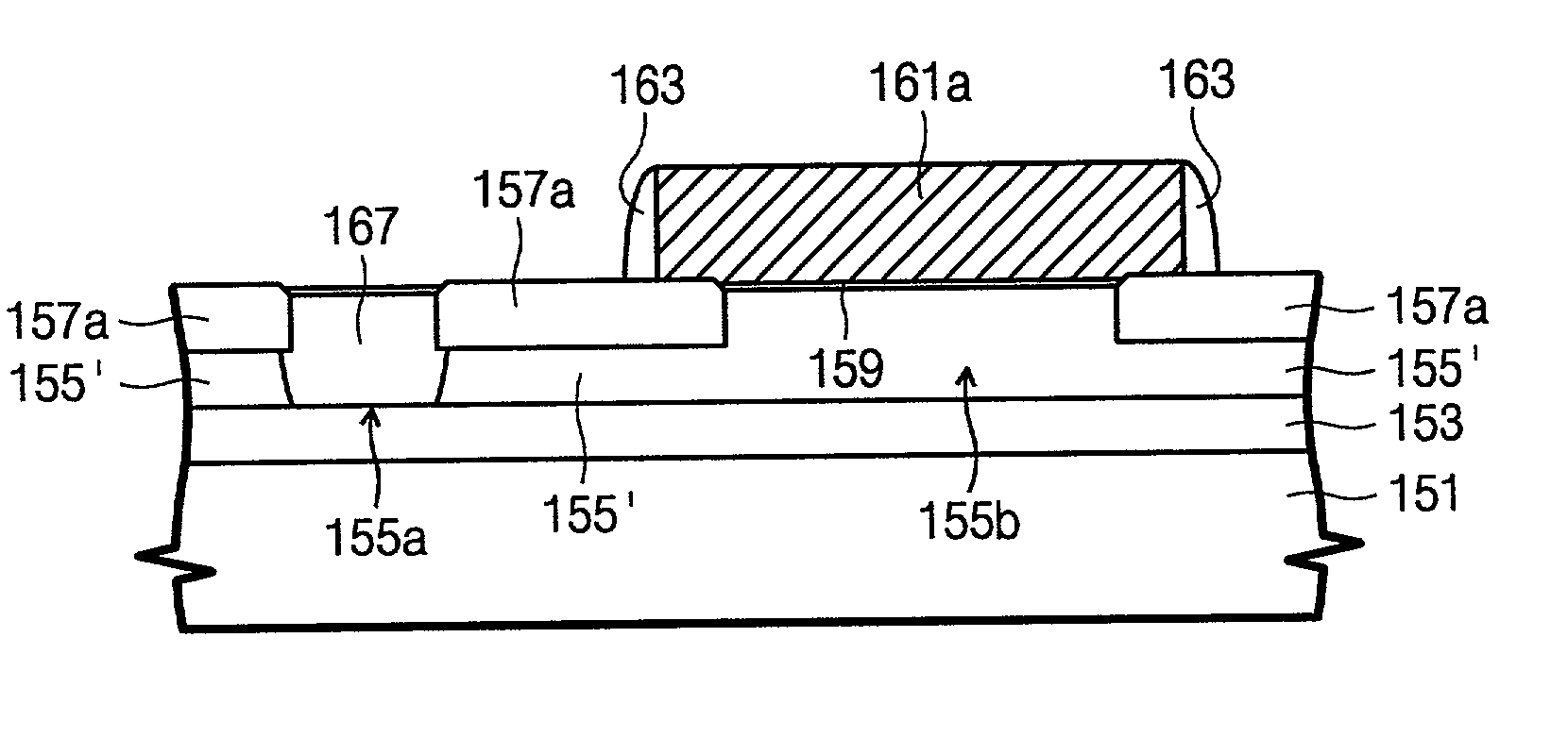
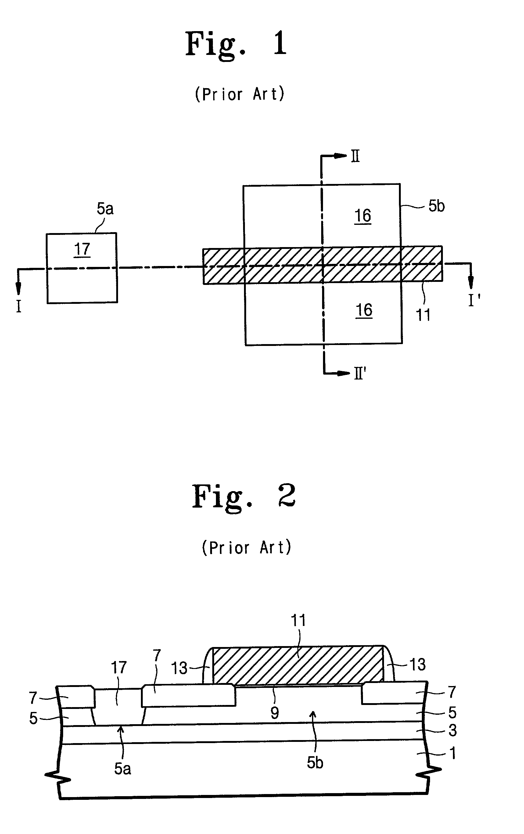
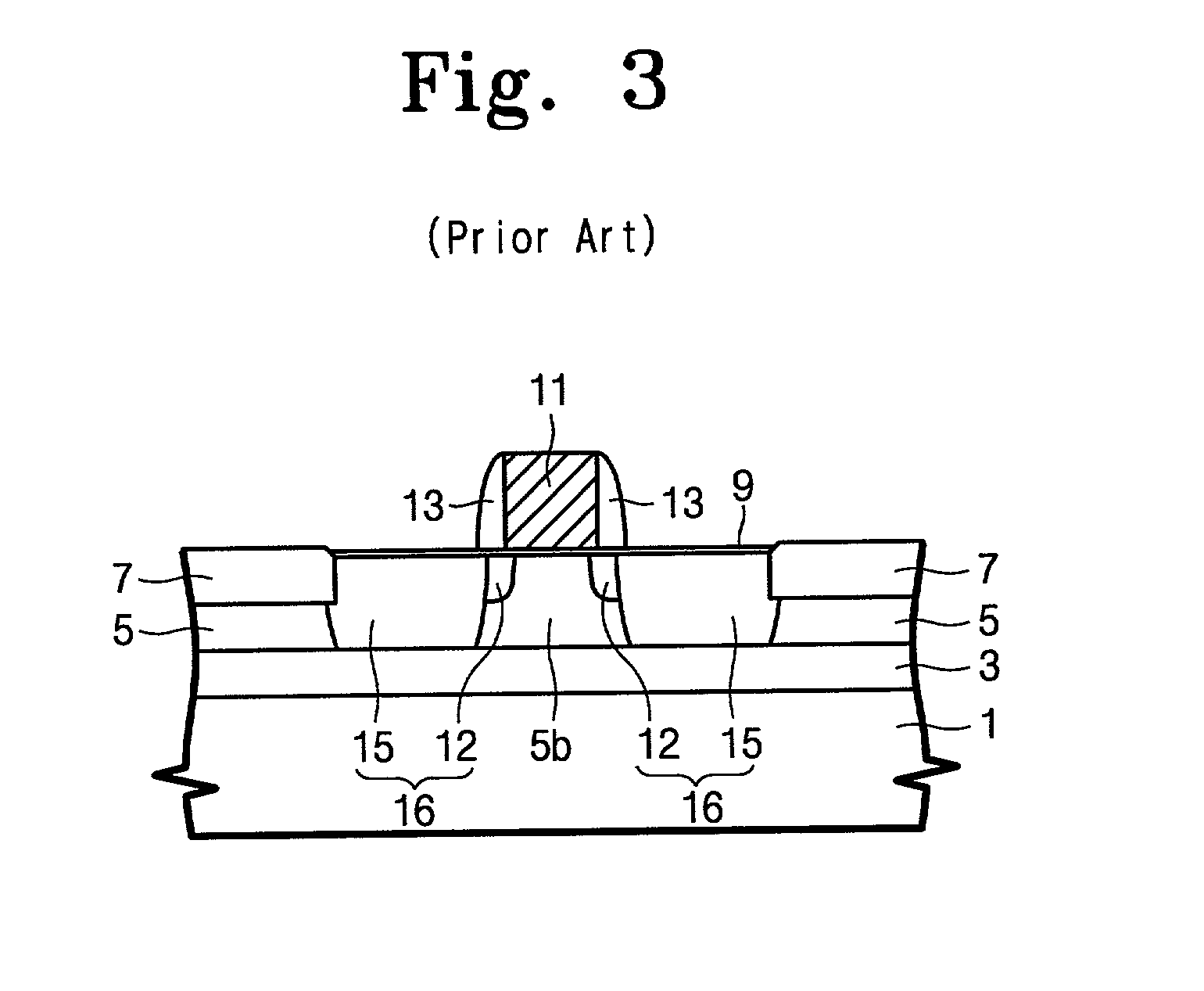
[0025] The present invention will be described in detail with reference to the accompanying drawings. Hereinafter, an SOI integrated circuit including N-MOSFETs or P-MOSFETs will be described with reference to the accompanying drawings. However, the present invention is applicable to SOI integrated circuits including CMOS circuits composed of P-MOSFETs and N-MOSFETs.

[0026] FIG. 4 is a top plan view showing an SOI integrated circuit according to one embodiment of the present invention. Also, FIG. 5 is a cross-sectional view taken along the line III-III' of FIG. 4 for illustrating an SOI integrated circuit according to the present invention, and FIG. 6 is a cross-sectional view taken along the line IV-IV' of FIG. 4 for illustrating an SOI integrated circuit according to the present invention.

[0027] Referring to FIGS. 4, 5 and 6, a partial trench isolation layer 157a is formed at a predetermined region of a semiconductor layer having a first conductivity type. The first conductivity ty...


PUM


Abstract

A silicon-on-insulator (SOI) integrated circuit and a method of fabricating the SOI integrated circuit are provided. A plurality of transistor active regions and at least one body contact active region are formed on an SOI substrate. A semiconductor residue layer, which is thinner than the transistor active regions and the body contact active region, is disposed between the transistor active regions and the body contact active region. The transistor active regions, the body contact active region and the semiconductor residue layer are disposed on a buried insulating layer of the SOI substrate. The semiconductor residue layer is covered with a partial trench isolation layer. A bar-shaped full trench isolation layer is interposed between the adjacent transistor active regions. The full trench isolation layer is in contact with sidewalls of the transistor active regions adjacent thereto and is in contact with the buried insulating layer between the adjacent transistor active regions. An insulated gate pattern crosses over the respective transistor active regions. The insulated gate pattern is disposed to be parallel with the full trench isolation layer.

Description

[0001] This application relies for priority upon Korean Patent Application No. 2001-05976, filed on Feb. 7, 2001, the contents of which are herein incorporated by reference in their entirety.[0002] The present invention generally relates to silicon-on-insulator (SOI) technology, and more particularly to an SOI semiconductor integrated circuit for eliminating floating body effects in SOI MOSFETs and a method of fabricating the same.DESCRIPTION OF THE RELATED ART[0003] In the semiconductor manufacturing industry, there has been a great deal of attention paid to reducing parasitic capacitance and resistance to increase the operating speed of semiconductor integrated circuits. SOI MOSFETs have been demonstrated to be superior to bulk silicon MOSFETs in terms of low power, high speed very large scale integration (VLSI) applications because of their inherent merits such as less junction capacitance and better device isolation. In addition, there are many advantages in SOI devices such as ...

Claims


Application Information

Patent Timeline
IPC IPC(8): H01L27/08H01L21/336H01L21/76H01L21/8238H01L27/092H01L27/12H01L29/786
CPCH01L27/1203H01L29/66772H01L29/78615H01L29/78621H01L21/76
Inventor LEE, SOO-CHEOLLEE, TAE-JUNG
Owner SAMSUNG ELECTRONICS CO LTD
Why Eureka
Eureka Blog
Learn More