This presumption is not always realistic.
Presently, there is no adequate technique for analyzing delays due to such factors as low probability
coupling between adjacent
signal lines within a circuit, or due to manufacturing steps that are imperfect but not so serious as to cause an outright failure.
Such manufacturing imperfections, or defects, may occur due to effects in newer technologies such as partially-depleted
silicon-on-insulator (PD-SOI) where elements such as the bodies of transistors are floating rather than being electrically connected to any other node or the
chip substrate.
Changes in the
voltage of such floating elements cause changes in threshold voltages, which in turn cause shifts in circuit delays.
A class of defects is suspected of causing these floating elements to have higher leakage current, which can shift the balance of body currents and thereby shift the body
voltage and the circuit delays.
Newer technologies such as partially-depleted
silicon-on-insulator (PD-SOI) have floating elements susceptible to such defects.
This type of
delay defect may have been present in older bulk technologies, but because such technologies did not have floating body elements, did not cause sufficient
delay shifts to be noticeable.
Thus, conventional static timing analysis techniques do not account for such
circuit delay shifts except in very simplistic ways.
Moreover, there has been no tool that can help a designer in such situations to isolate timing bottlenecks due to such delay shifts and make design decisions before circuit fabrication.
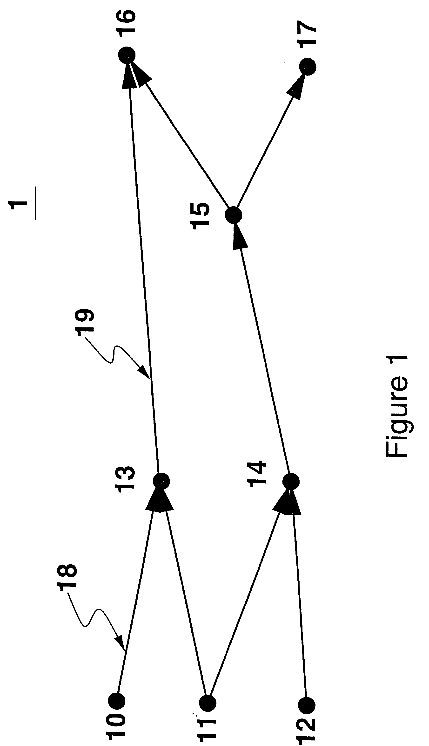
Delays in a
logic network may not be exactly knowable, due to variations in the manufacture of the
integrated circuit(s) in which the
logic network is implemented, and due to various details of the design which, though theoretically predictable, are ignored (due to
processing time limitations or inadequate modeling) in delay calculations.
Defects in the circuit comprising a logic network can also cause variations in the delays of the network.
In the past most defects which affected delays were likely to reduce the reliability of the network, and there was therefore no incentive to accommodate them in static timing analysis.
Examples of such faults are
high resistance connections due to narrowed conductors or incompletely filled vias.
With the introduction of partially-depleted of
silicon-on-insulator (PD-SOI) technology it appears that there may be a class of defects which affects
circuit delay but which does not otherwise affect the reliability or functioning of the circuit.
This body
voltage variation causes a shift in the
threshold voltage of the transistors, which in turn causes a variation in the circuit delays.
It appears that there may be a class of process defect which causes increased leakage of the source and drain
diode junctions in a device.
Such defects may have been present in past bulk technologies, but because the change in leakage caused is very small, and because the device bodies in these technologies were tied to ground (for NFETs) or Vdd (for PFETs), they would have had a negligible effect on device performance.
In PD-SOI technologies, however, such increased leakage could shift the balance of body currents in a device, affecting the body voltage of the device and hence the delay of the circuit.
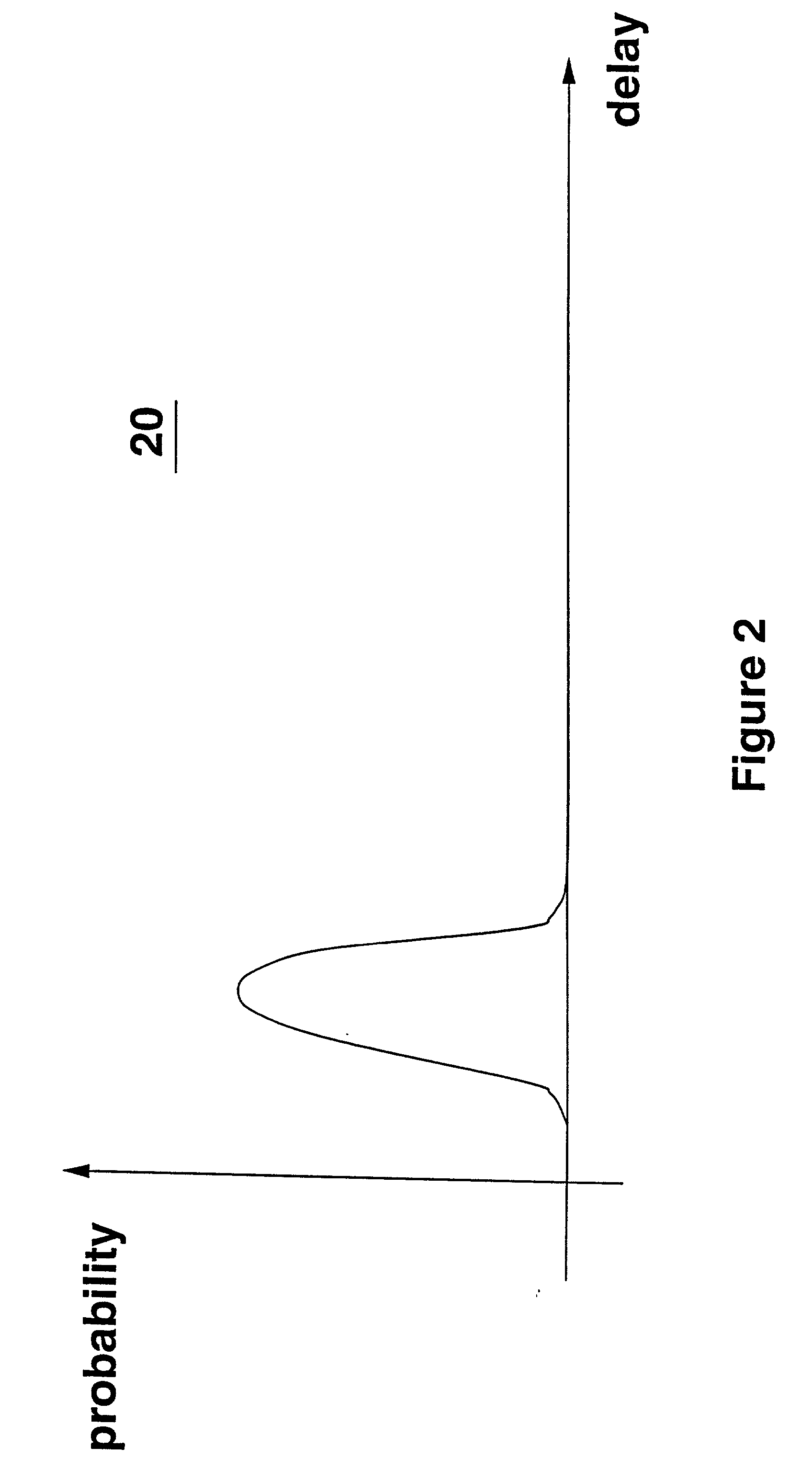
However the probability that it would occur somewhere on a
chip could be significant (there is speculation that perhaps one fourth of all chips exhibit such defects).
Typically, under normal operation this tighter
coupling does not present a problem, but with ever tighter pitches between conductors, the chance becomes greater for significant shifts in time delay due to coupling between simultaneously transitioning conductors. . Techniques are known in the art to compute the delay shift due to such coupling when it occurs, but because the exact alignment of transitions in adjacent conductors is rare, it is pessimistic to assume that all pairs of adjacent conductors always exhibit such a delay shift.
The conventional techniques do not fully address the problems with infrequently occurring coupling delays.
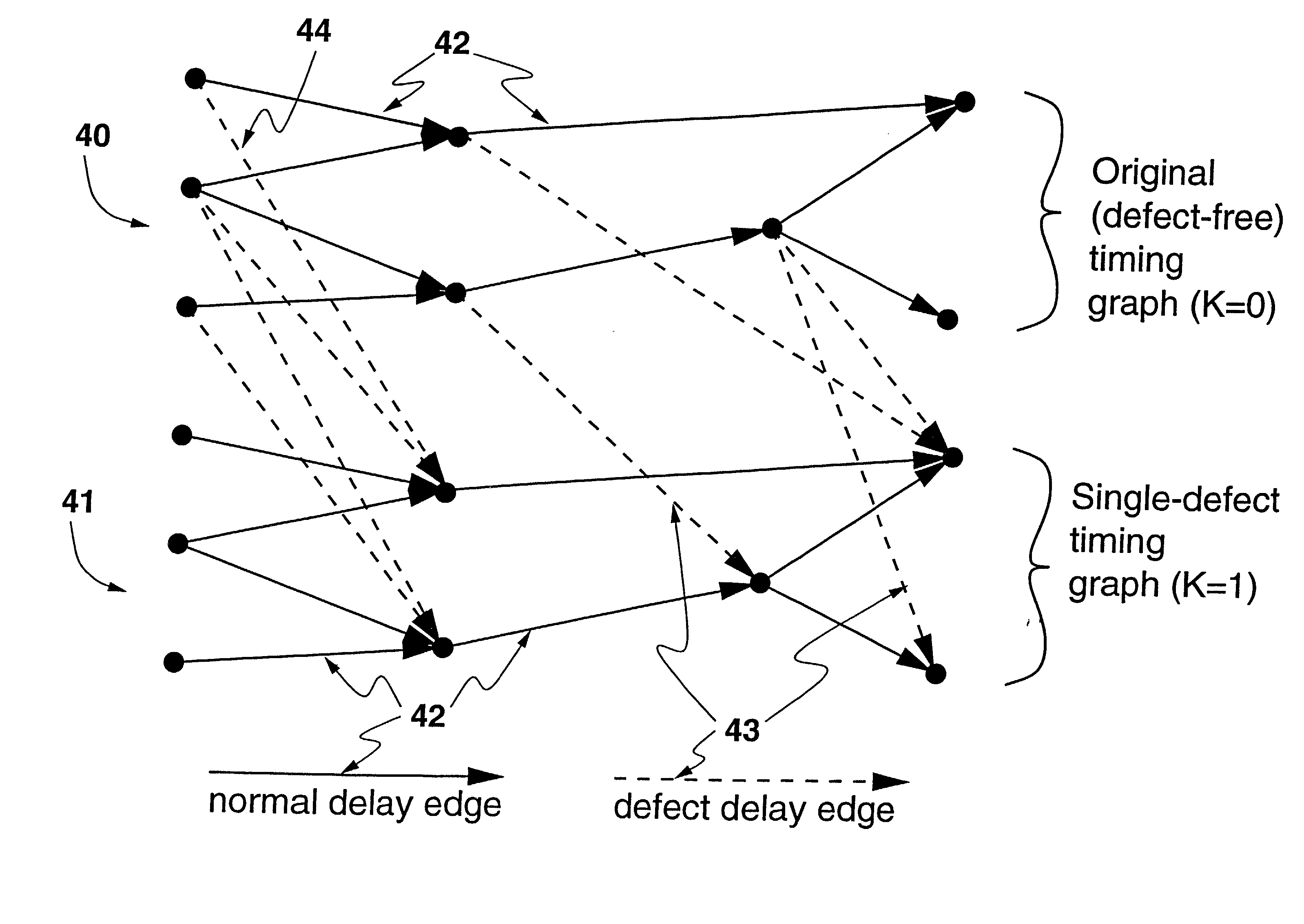
Because these types of defect may cause a significant shift in
circuit delay but may occur only rarely, past methods for modeling delay variation in static timing analysis are inadequate for modeling the effects of such defects.

