Method for fabricating ultra high-resistive conductors in semiconductor devices and devices fabricated

Inactive Publication Date: 2002-09-12
IBM CORP
View PDF0 Cites 4 Cited by
  • Summary
  • Abstract
  • Description
  • Claims
  • Application Information

AI Technical Summary

Benefits of technology

0013] In accordance with the present invention, a high density resistor structure and a method for forming the high density resistor structure are disclosed.
0014] In a preferred embodiment, a high density resistor structure is provided which includes an electrically insulated substrate that has a top surface; a refractory metal-silicon-nitrogen layer deposited on the top surface; and at least one resistor element patterned in the refractory metal-silicon-nitrogen layer in a plane parallel to the top surface.
0015] In the high density resistor structure, the at least two resistor elements are electrically connected in series or in parallel. The electrically insulated substrate may be a semiconductor substrate, or a glass substrate. The refractory metal-silicon-nitrogen may be a member selected from the group consisting of TaSiN, NbSiN, VSiN and WSiN. The refractory metal-silicon-nitrogen layer may be deposited to a thickness between about 200 .ANG. and about 2000 .ANG., or preferably, to a thickness between about 300 .ANG. and about 700 .ANG.. The refractory metal-silicon-nitrogen layer may be TaSiN deposited to a thickness of about 500 .ANG..
0016] In the high density resistor structure, the refractory metal-silicon-nitrogen layer may be TaSiN containing between about 10 at % and about 55 at % Ta, between about 10 at % and about 45 at % Si, and between about 30 at % and about 80 at % N. The refractory metal-silicon-nitrogen layer may be TaSiN containing preferably between about 45 at % and about 80 at % N. The refractory metal-silicon-nitrogen layer may be TaSiN that has a she

Problems solved by technology

When semiconductor devices are fabricated, it is difficult to provide resistors in-situ in the semiconductor structure.
Particularly, it has not been possible to form resistors in-situ in the structure that provide high resistance in the range of more than several thousand .OMEGA. / sq.
Doped polysilicon resistors are known to have unstable material characteristics, due to a grain boundary effect, i.e. the resistivity will decrease when annealed due to grain growth.
One reason for such difficulty is the unavailability of a material that can be used in a semiconductor fabrication process which has sufficiently high electrical resistivity.

Method used


Image

  • Method for fabricating ultra high-resistive conductors in semiconductor devices and devices fabricated
  • Method for fabricating ultra high-resistive conductors in semiconductor devices and devices fabricated
  • Method for fabricating ultra high-resistive conductors in semiconductor devices and devices fabricated

Examples


Embodiment Construction

[0024] The present invention discloses a high density resistor structure that includes an electrically insulative substrate, either an insulated semiconductor substrate or a glass substrate which has a top surface; a refractory metal-silicon-nitrogen layer deposited on the top surface; and at least one resistor element patterned in the refractory metal-silicon-nitrogen layer in a plane parallel to the top surface.

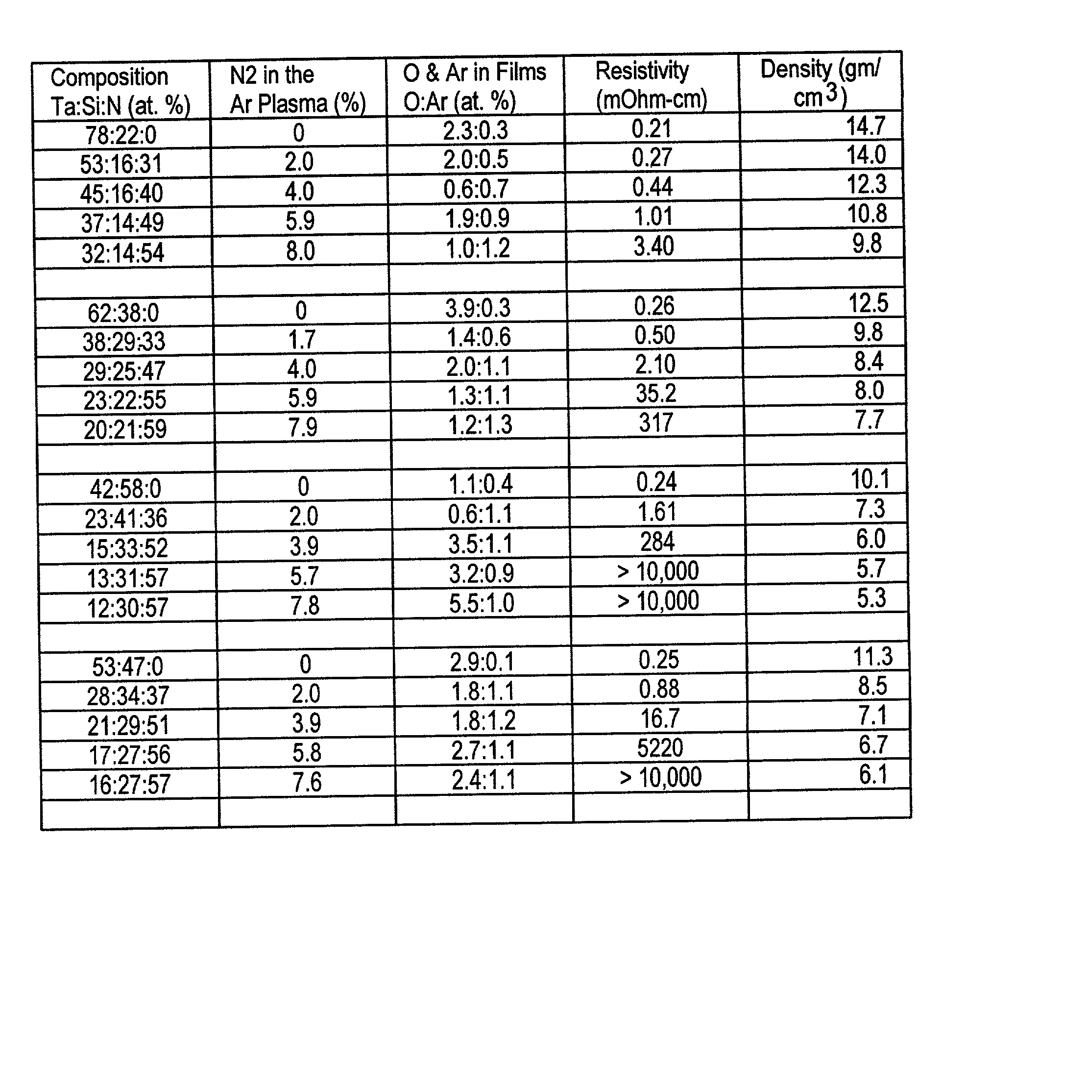
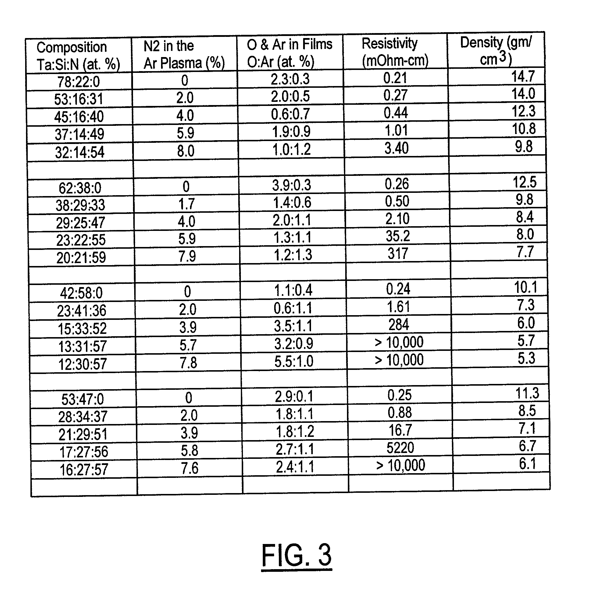
[0025] As shown in a preferred embodiment, TaSiN is used as the refractory metal-silicon-nitrogen deposited to a thickness between about 200 .ANG. and about 2000 .ANG., and preferably between about 300 .ANG. and about 700 .ANG.. In a typical application, the TaSiN composition may be formed of between about 10 at % and about 55 at % Ta, between about 10 at % and about 45 at % Si, and between about 30 at % and about 80 at % N; and preferably between about 45 at % and about 80 at % N. The refractory metal-silicon-nitrogen layer may be suitably deposited and then patterned into...


PUM


Abstract

A high density resistor structure and a method for forming the structure are disclosed. The high density resistor structure can be constructed by an electrically insulative substrate; a refractory metal-silicon-nitrogen layer deposited on the top surface; and at least one resistor element patterned in the refractory metal-silicon-nitrogen layer in a plane parallel to the top surface. The method can be carried out by first providing the electrically insulative semiconductor substrate or a glass substrate, then sputter-depositing a TaSiN layer having a thickness between 200 .ANG. and 2000 .ANG. on top of the substrate; and then forming by a reactive ion etching technique at least one resistor element in the TaSiN film in a plane that is parallel to the top surface of the substrate.

Description

FIELD OF THE INVENTION[0001] The present invention generally relates to a method for fabricating high-resistive conductors in semiconductor devices and devices formed and more particularly, relates to a method for fabricating ultra high-resistive conductors that are formed of refractory metal-silicon-nitrogen for use in semiconductor devices and devices formed.BACKGROUND OF THE INVENTION[0002] In the fabrication of electronic devices, resistors are connected to a circuit board for providing specific electrical resistances to an electronic circuit. When semiconductor devices are fabricated, it is difficult to provide resistors in-situ in the semiconductor structure. Particularly, it has not been possible to form resistors in-situ in the structure that provide high resistance in the range of more than several thousand .OMEGA. / sq. The only in-situ formed resistor designed for use in a semiconductor device has been a diffusion resistor that is normally formed on the surface of a substra...

Claims


Application Information

Patent Timeline
IPC IPC(8): H01C17/12H01L21/02H01L27/08
CPCH01C17/12H01L27/0802H01L28/24
Inventor CABRAL, CYRIL JR.CLEVENGER, LAWRENCEHSU, LOUIS LU-CHENWONG, KEITH KWONG HON
Owner IBM CORP
Why Eureka
Try Eureka