

Method for manufacturing device substrate with metal back-gate and structure formed thereby
a technology of metal back-gate and device substrate, which is applied in the direction of semiconductor devices, electrical devices, transistors, etc., can solve the problem of stacked layers being very likely to disintegra
- Summary
- Abstract
- Description
- Claims
- Application Information
AI Technical Summary
Benefits of technology
Problems solved by technology
Method used
Image

Examples
Embodiment Construction
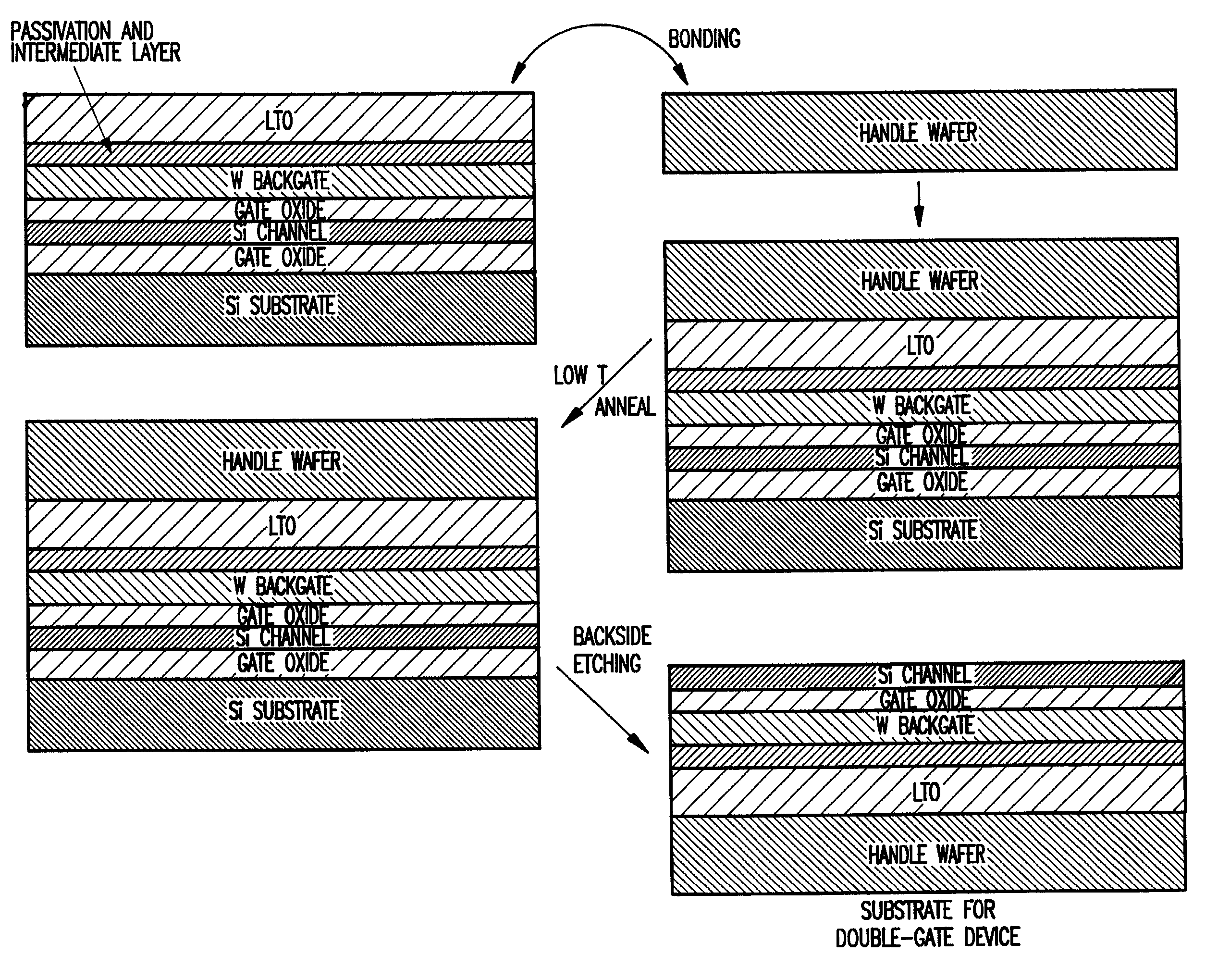
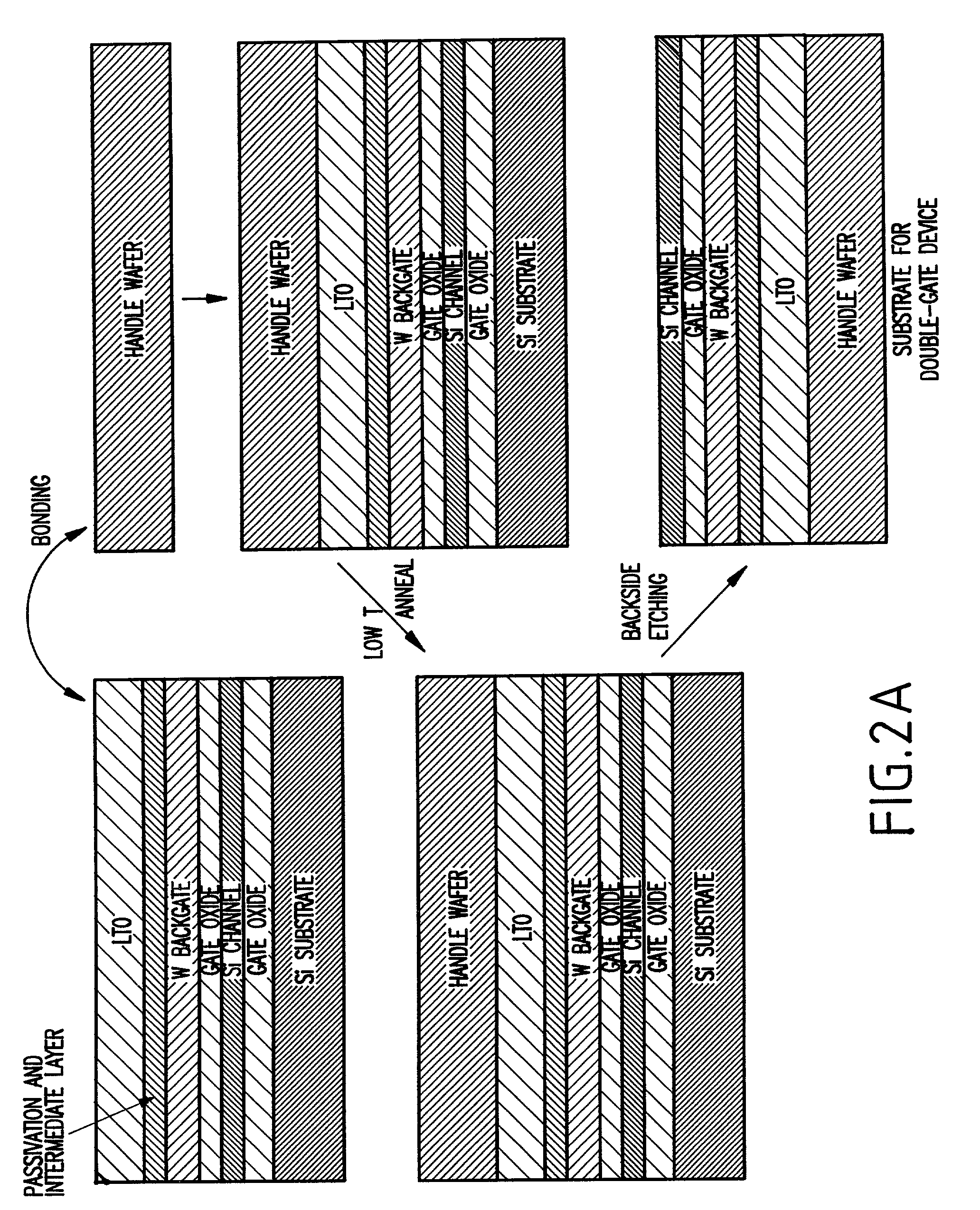
[0019] Referring now to the drawings, and more particularly to FIGS. 2-5, there are shown preferred embodiments of the method and structures according to the present invention.
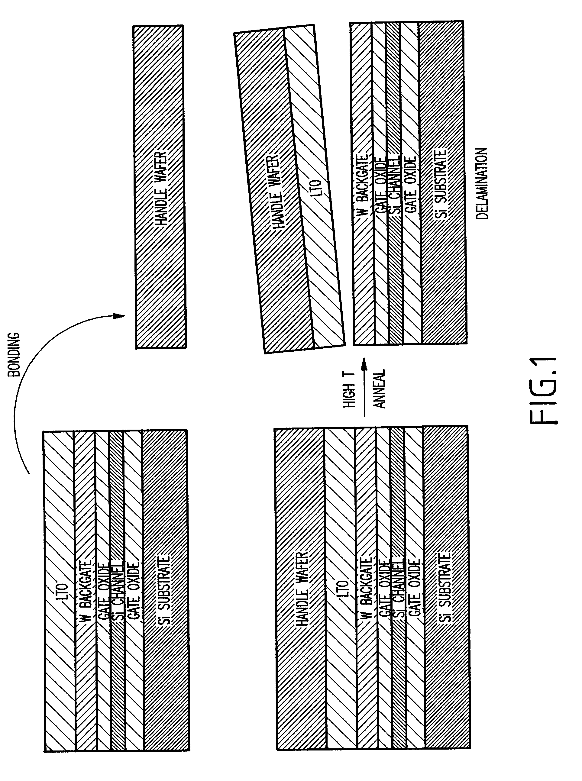
[0020] As mentioned above, the present invention resolves the above-mentioned and other problems of delamination between metals (e.g., W, TiN, etc.; W will be assumed in the example described below) and low temperature oxide (LTO) during bonding anneal by improving the adhesion between these two incompatible materials with several innovative processes. As such, an 8" device substrate with W as the back-plane has been demonstrated for the first time, as shown in FIG. 4 which is a photograph of the 8" device substrate.
[0021] A key aspect of the method of the present invention is to use an intermediate "gluing" layer to enhance adhesion between multi-layers especially two layers with very different chemical and physical properties.
[0022] It is noted that this aspect can be well extended from a W back-gate to othe...
PUM
| Property | Measurement | Unit |
|---|---|---|
| pressure | aaaaa | aaaaa |
| temperatures | aaaaa | aaaaa |
| thickness | aaaaa | aaaaa |
Abstract
Description
Claims
Application Information