Contact structure with a lower interconnection having t-shaped portion in cross section and method for forming the same

a contact structure and interconnection technology, applied in the direction of semiconductor devices, semiconductor/solid-state device details, electrical equipment, etc., can solve the problems of non-uniform resistance values, many problems, and serious global step difference problems

Inactive Publication Date: 2002-10-24
SAMSUNG ELECTRONICS CO LTD
View PDF0 Cites 63 Cited by
  • Summary
  • Abstract
  • Description
  • Claims
  • Application Information

AI Technical Summary

Problems solved by technology

This global step difference causes many problems during a subsequent metal wiring process.
In particular, in the case of a Merged DRAM with Logic (MDL) device, the number of layers of a

Method used


Image

  • Contact structure with a lower interconnection having t-shaped portion in cross section and method for forming the same
  • Contact structure with a lower interconnection having t-shaped portion in cross section and method for forming the same
  • Contact structure with a lower interconnection having t-shaped portion in cross section and method for forming the same

Examples


Embodiment Construction

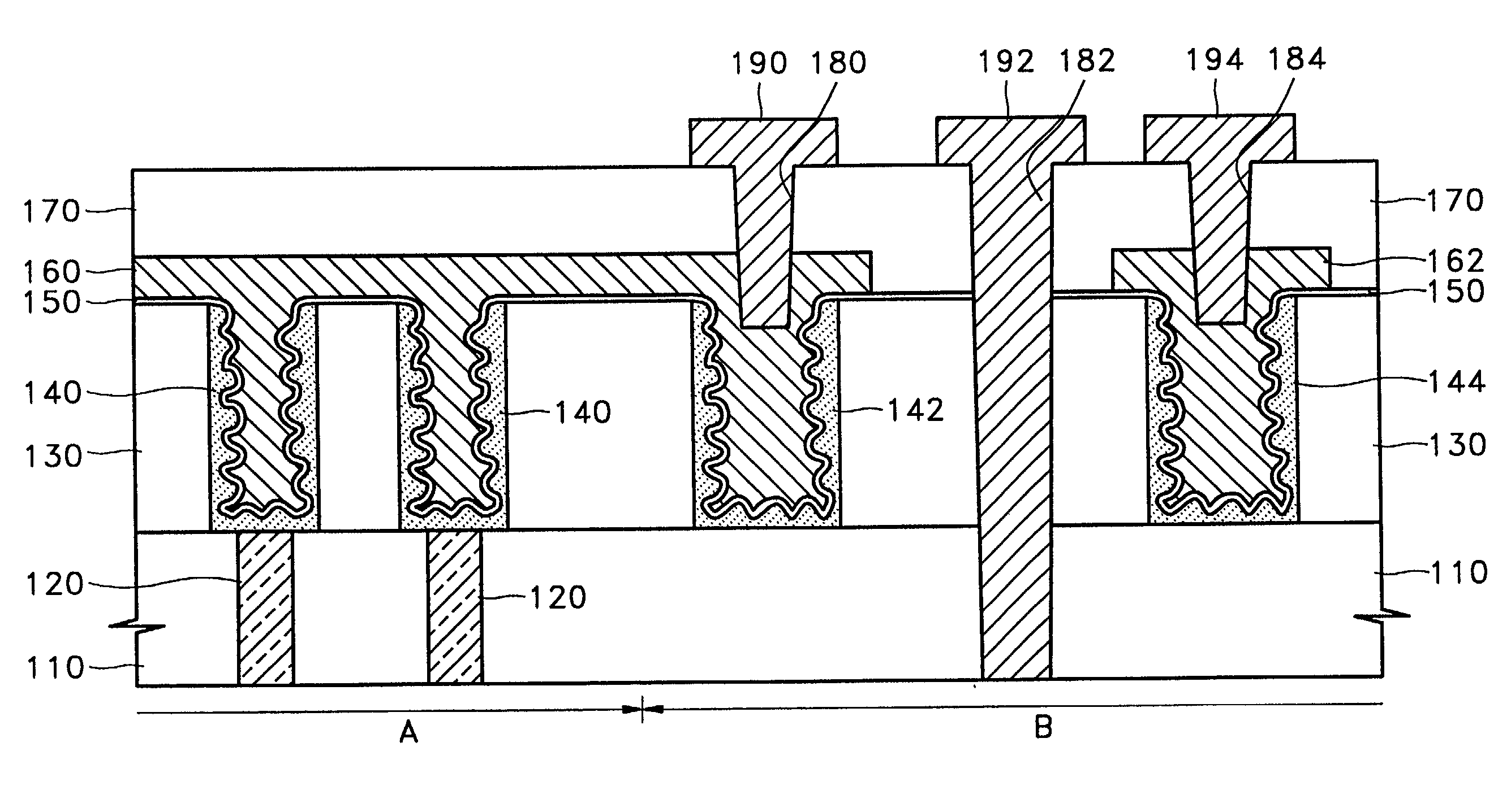
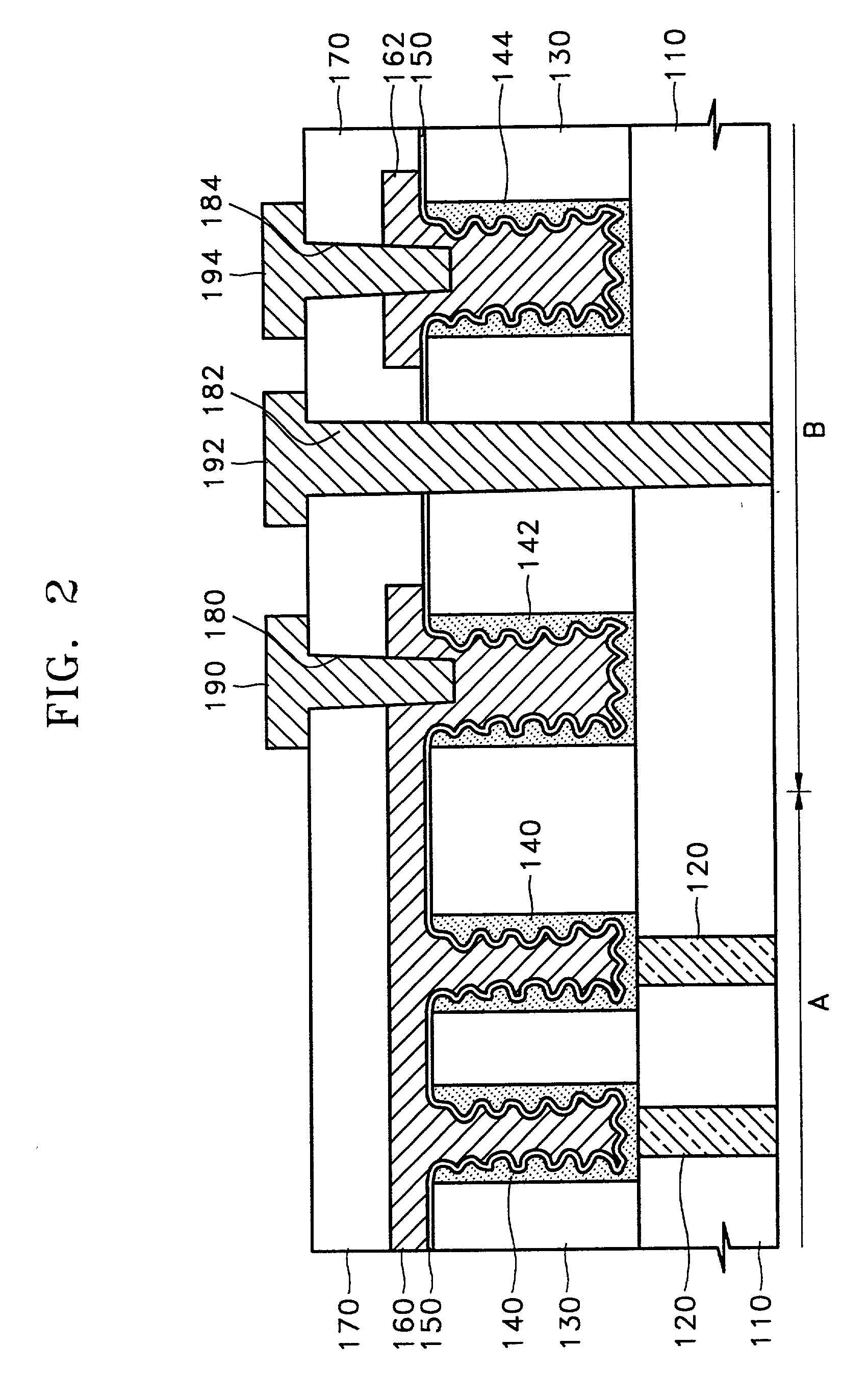
[0018] Hereinafter, embodiments of the present invention will be described in detail with reference to the attached drawings. The present invention is not restricted to the following embodiments, and many variations are possible within the sprit and scope of the present invention. In the drawings, the shapes of some members are exaggerated for clarity and the same reference numerals denote the same members. Also, when a layer is described as being on another layer, it can be directly on the other layer or an interlayer film can exist therebetween.

[0019] FIG. 2 is a partial, cross-sectional view of a semiconductor device including a dynamic random access memory (DRAM) having a contact structure according to an embodiment of the present invention. Referring to FIG. 2, the semiconductor device of this embodiment is composed of a cell array area A in which a plurality of DRAM cells are formed to the left in the drawing and a peripheral circuit area or a logic circuit area B including co...


PUM


Abstract

A contact structure in a semiconductor device including a dynamic random access memory (DRAM) and a method of forming the same are provided. The contact structure, which is formed in a peripheral circuit area or a logic circuit area of a semiconductor device including a DRAM having a cell array area with a plurality of DRAM cells and the peripheral or logic circuit area, includes a lower interconnection formed of the same material as a capacitor upper electrode of each of the plurality of DRAM cells; an interlayer dielectric layer formed on the lower interconnection and having a contact hole exposing a predetermined portion of the lower interconnection; and an upper interconnection formed on the interlayer dielectric layer and electrically connected to the lower interconnection through the contact hole. The lower portion of the lower interconnection has a larger area than the bottom of the contact hole and extends downward so that the lower interconnection has a T-shape in a cross-section view. By forming the lower interconnection under a shallow contact hole to have a T-shape extending downward when forming contact holes having a large difference in depth, the lower interconnection can be prevented from being pierced when the contact holes are formed. Consequently, stable and uniform contact resistance can be obtained.

Description

[0001] 1. Field of the Invention[0002] The present invention relates to a semiconductor device, and more particularly, to a contact structure in a semiconductor device including a dynamic random access memory (DRAM) with a capacitor, and a method of forming the same.[0003] 2. Description of the Related Art[0004] As the integration density of semiconductor devices increases, the area of a capacitor, which is an information storage unit of a memory device, e.g. DRAM, decreases. To obtain capacitance equal to or lager than that before on the decreased area, methods for increasing the area of an effective electrode by making the electrode of the capacitor in a three-dimensional shape such as a cylinder or a pin have been used. However, as the height of an electrode of a capacitor increases, a global step difference between a cell array area in which the capacitor is formed and a peripheral circuit area or a logic circuit area for driving memory cells increases. This global step differen...

Claims


Application Information

Patent Timeline
IPC IPC(8): H01L21/768H01L23/522H01L21/8242H01L27/108
CPCH01L21/76802H01L27/10894H01L27/10882H01L27/10814H10B12/315H10B12/48H10B12/09H10B99/00
Inventor OH, JAE-HEE
Owner SAMSUNG ELECTRONICS CO LTD
Why Eureka
Try Eureka