Method for forming a copper thin film

a thin film and copper technology, applied in the direction of superimposed coating process, plasma technique, coating, etc., can solve the problems of fatal defect in high speed device manufacturing, increase in wiring resistance, and reduction of electro-migration resistance or the lik

Inactive Publication Date: 2002-10-31
ANELVA CORP
View PDF0 Cites 12 Cited by
  • Summary
  • Abstract
  • Description
  • Claims
  • Application Information

AI Technical Summary

Problems solved by technology

When the Cu thin film thus formed is used as wiring, there occurs a drawback such as increase in wiring resistance, reduction in electro-migration resistance or the like.
As described above, however, if the wiring resistance is increased due to the existence of fine voids in the vicinity of the interface between the first copper film (Cu-Seed film), which is in the as depo. state, and the second copper film formed thereon by the electrolytic copper plating, such increase may result in a fatal defect in manufacturing of a high speed device.
So that, reduction in electro-migration resistance also may result in a fatal defect in manufacturing of a high speed device.

Method used


Image

  • Method for forming a copper thin film
  • Method for forming a copper thin film
  • Method for forming a copper thin film

Examples


Embodiment Construction

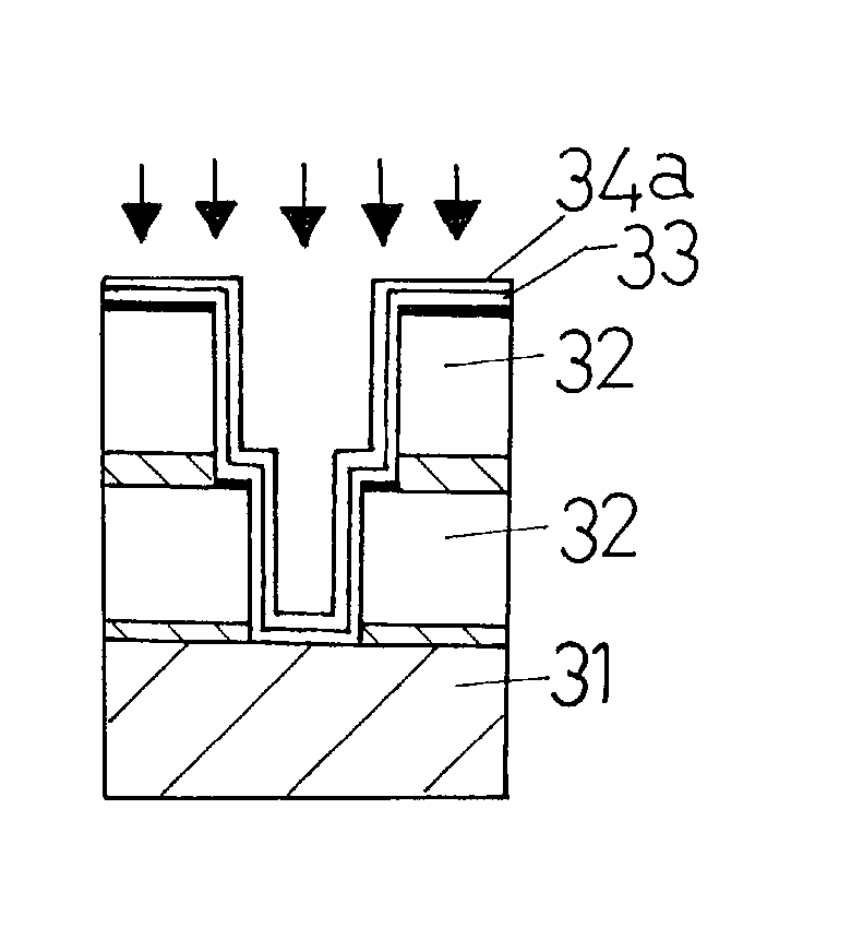
[0057] Regarding a sample substrate which was obtained by further forming the second copper film 35 on the first copper film 34 by the electrolytic copper plating process using the first copper film 34 (Cu-Seed film 34a) as an electrode, the section of the film of the sample substrate which was plated was observed with a SEM (scanning electron microscope). The said first copper film 34(Cu-seed film 34a) has been modified through the above-described process. A sample substrate which was subjected to a modification process using plasma of Ar gas and a sample substrate which was subjected to a modification process using plasma of Ar gas mixed with H.sub.2 gas were observed with the same magnification as the conventional case shown in FIGS. 3 and 4. In both the sample substrates, it was not found that any void existed in the vicinity of the interface between the first copper film (Cu-Seed film) and the second copper film formed thereon by the electrolytic copper plating process.

[0058] R...


PUM

PropertyMeasurementUnit
temperatureaaaaaaaaaa
pressureaaaaaaaaaa
flow rateaaaaaaaaaa

Abstract

In a method for forming a Cu thin film on a substrate including a Cu-CVD step of forming a first copper film on predetermined surface of a substrate by a CVD process and a plating step of further forming a second copper film on the first copper film by an electrolytic copper plating process using the first copper film as an electrode, a modifying step for modifying the first copper film by exposing it in an active atmosphere is interposed between the Cu-CVD step and the plating step. Thereby, fine voids can be effectively prevented from being formed in the vicinity of the interface between the first copper film and the second copper film.

Description

[0001] 1. Field of the Invention[0002] The present invention relates to a method for forming a Cu thin film, and in particular, to a method for forming a Cu thin film suitable for forming a Cu thin film for wiring, where a copper film is formed on a diffusion barrier film formed on an insulating film formed on a substrate to be processed and provided with a recessed portion, and the recessed portion is filled with copper material.[0003] 2. Description of the Related Art[0004] In recent years, according to high performance orientation of semiconductor devices, Cu (copper) has been used as wiring material. The reason is that Cu has a lower electrical resistance than that of Al (aluminum), and Cu has a high resistance to a phenomenon such as stress-migration and electro-migration where diffusion behavior of metal atoms constituting wiring is dominant.[0005] In forming a wiring using Cu, a pattern of wiring and connection hole (via hole, or contact hole) is formed on an insulating film,...

Claims


Application Information

Patent Timeline
Patent Type & Authority Applications(United States)
IPC IPC(8): C23C16/18C25D5/34C23C28/02C25D7/12H01L21/28H01L21/285H01L21/288H01L21/768
CPCC23C28/023H01L21/28556H01L21/2885H01L21/76877H01L21/76864H01L21/76873H01L21/76862
Inventor SEKIGUCHI, ATSUSHISHIBAGAKI, MASAMIKOIDE, TOMOAKIKUNINOBU, TAKAFUMISUZUKI, KAORU
Owner ANELVA CORP
Why Eureka
Try Eureka