Polishing pad for semiconductor wafer and laminated body for polishing of semiconductor wafer equipped with the same as well as method for polishing of semiconductor wafer

a technology of semiconductor wafers and laminated bodies, which is applied in the direction of flexible parts wheels, manufacturing tools, flexible parts, etc., can solve the problems of ineffective polishing of different polishings, inability to obtain all polishing times, and inability to achieve essential ability, so as to achieve effective polishing, reduce the polishing performance of polishing, and facilitate optical detection of polishing endpoints

Inactive Publication Date: 2002-11-21
JSR CORPORATIOON
View PDF0 Cites 47 Cited by
  • Summary
  • Abstract
  • Description
  • Claims
  • Application Information

AI Technical Summary

Benefits of technology

0027] According to the polishing pad for a semiconductor wafer of the first and second aspects of the invention and the laminated body for polishing of a semiconductor wafer equipped with the same, optical detection of a polishing endpoint can be easily performed without lowering the polishing performance in polishing. In particular, according to the polishing pad of the first aspect of the invention, not only a polishing endpoint but also the all polishing situations can be always observed optically during polishing.
0028] According to the method for polishing of a semiconductor wafer of the invention, the semiconductor wafer can be effectively polished while observing the polishing situation, and the semiconductor wafer is not polished excessively.
0029] The polishing pad for a semiconductor wafer (hereinafter also referred to as "polishing pad") of the first aspect of the invention is characterized in that it is comprised of a water-insoluble matrix material and a water-soluble particle dispersed in the above-me...

Problems solved by technology

For this reason, it is so inefficient to obtain all polishing times in a variety of different polishings.
This window has no polishing ability, and has no essential ability such as absorption and transportation of slurry particles.
However, since the window in the above-mentioned polishing pad has no polishing ability, there is a possibility that pr...

Method used


Image

  • Polishing pad for semiconductor wafer and laminated body for polishing of semiconductor wafer equipped with the same as well as method for polishing of semiconductor wafer
  • Polishing pad for semiconductor wafer and laminated body for polishing of semiconductor wafer equipped with the same as well as method for polishing of semiconductor wafer
  • Polishing pad for semiconductor wafer and laminated body for polishing of semiconductor wafer equipped with the same as well as method for polishing of semiconductor wafer

Examples


example 2

[0135] Using a polishing pad composed of commercially available polyurethane foam having no light transmitting properties (trade name "IC1000" manufactured by Rodel Nitta), polishing was performed under the same conditions as those of Example 1, and a removal rate was 950 .ANG. / min. A circular through hole having a diameter of 20 mm was provided on this polishing pad, and a light transmitting part having the same constituent as that of the polishing pad in the above-mentioned Example 1 was fitted therein. Polishing was performed under the same conditions as those of Example 1 using this new polishing pad, and a removal rate was 950 .ANG. / min.

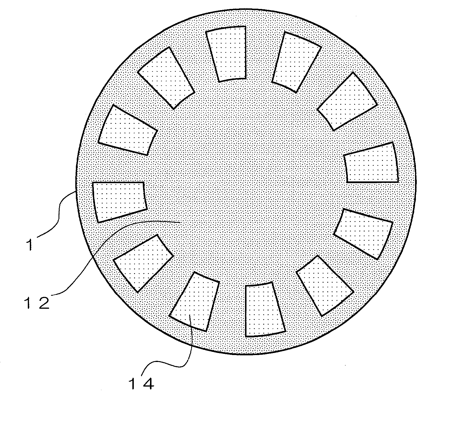
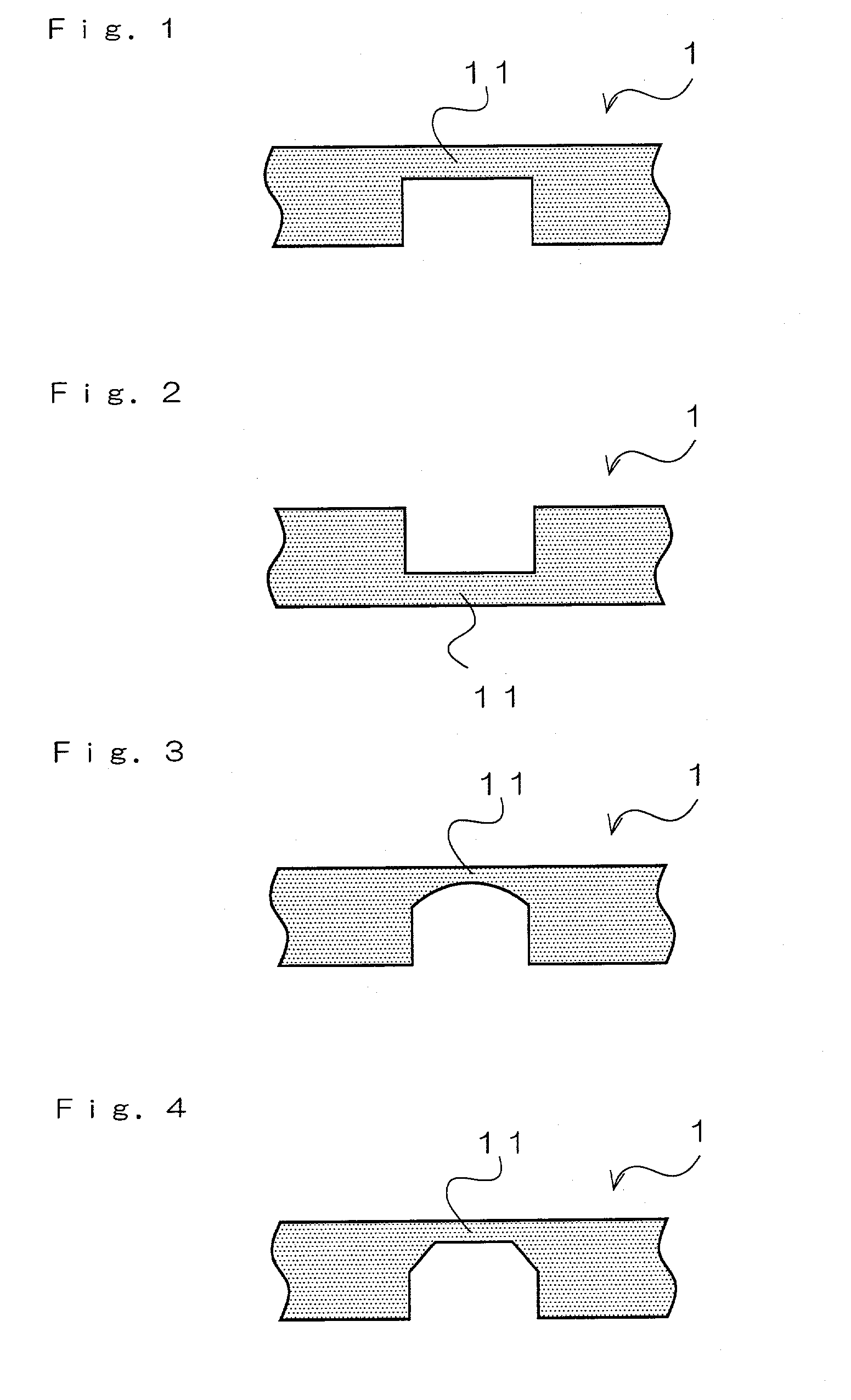
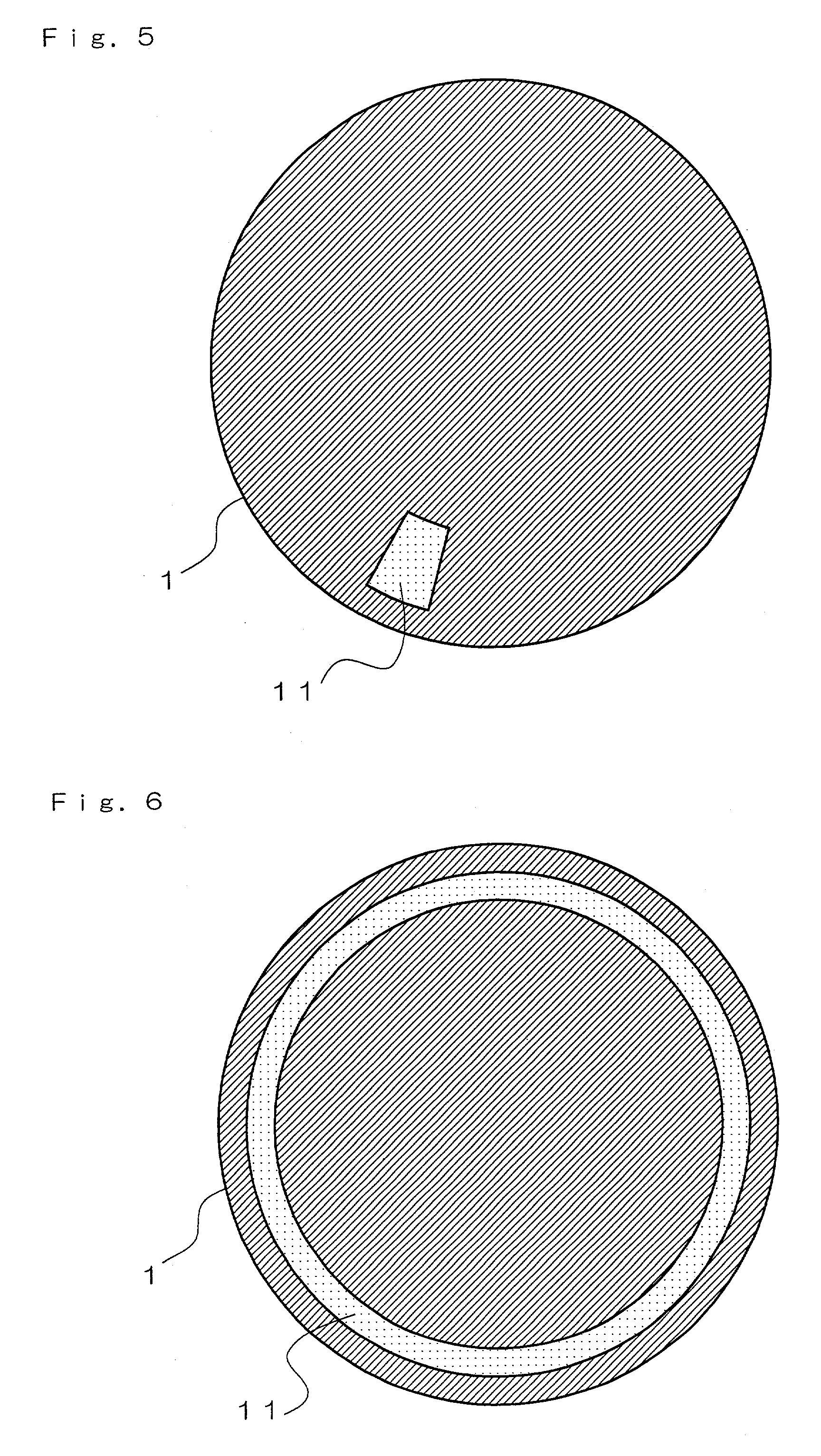
[0136] As a result, even when, a light transmitting part molded in a prescribed size is fitted in a through hole provided on a part of a polishing pad composed of polyurethane foam having no light transmitting properties to obtain a polishing pad, which is used to perform polishing, it can be seen that the polishing performance of a polishing pa...


PUM

PropertyMeasurementUnit
Wavelengthaaaaaaaaaa

Abstract

An objective of the present invention is to provide a polishing pad for a semiconductor wafer and a laminated body for polishing of a semiconductor wafer equipped with the same which can perform optical endpoint detection without lowering the polishing performance as well as methods for polishing of a semiconductor wafer using them. The polishing pad of the invention comprises a water-insoluble matrix material such as crosslinked 1,2-polybutadiene, and a water-soluble particle such as beta-cyclodextrin dispersed in this water-insoluble matrix material, and has a light transmitting properties so that a polishing endpoint can be detected with a light.

Description

[0001] The present invention relates to a polishing pad for a semiconductor wafer and a laminated body for polishing of a semiconductor wafer equipped with the same as well as methods for polishing of a semiconductor wafer. More particularly, the present invention relates to a polishing pad for a semiconductor wafer through which the light can transmit and detection of a polishing endpoint with the transmitted light is easy without decreasing the polishing performance, and a laminated body for polishing of a semiconductor wafer equipped with the same as well as methods for polishing of a semiconductor wafer.DESCRIPTION OF THE PRIOR ART[0002] In polishing of a semiconductor wafer, determination of a polishing endpoint at which polishing is performed can be known based on the criteria of the empirically obtained time. However, there are a variety of materials constituting the surface to be polished, and polishing times are all different depending upon the materials. In addition, mater...

Claims


Application Information

Patent Timeline
IPC IPC(8): H01L21/304B24B37/013B24B37/20B24D3/34B24D7/12B24D13/12B24D13/14
CPCB24B37/013B24D13/12B24D3/344B24B37/205H01L21/304
Inventor HASEGAWA, KOU
Owner JSR CORPORATIOON
Why Eureka
Try Eureka