Method and apparatus for transferring a semiconductor substrate

a technology of semiconductor substrates and methods, applied in lighting and heating apparatus, charge manipulation, furniture, etc., can solve the problems of increased substrate throughput, increased cluster tool hardware and software costs, and undesirable use of dedicated orientation chambers

Inactive Publication Date: 2002-12-19
APPLIED MATERIALS INC
View PDF0 Cites 95 Cited by
  • Summary
  • Abstract
  • Description
  • Claims
  • Application Information

AI Technical Summary

Benefits of technology

0023] To facilitate understanding, identical reference numerals have been used, wherever possible, to designate identical elements that are common to the figures.

Problems solved by technology

Although the use of a dedicated orientation chamber coupled to the cluster tool has traditionally provided a robust process for determining the orientation of a substrate, the demand in the semiconductor industry for reduced cost of tool ownership and increased substrate throughput has made the use of a dedicated orientation chamber undesirable.
For example, a dedicated orientation chamber increases the cluster tool hardware and software cost.
Additionally, the use of a dedicated orientation chamber requires a time expenditure that is not directly related to processing.

Method used


Image

  • Method and apparatus for transferring a semiconductor substrate
  • Method and apparatus for transferring a semiconductor substrate
  • Method and apparatus for transferring a semiconductor substrate

Examples


Embodiment Construction

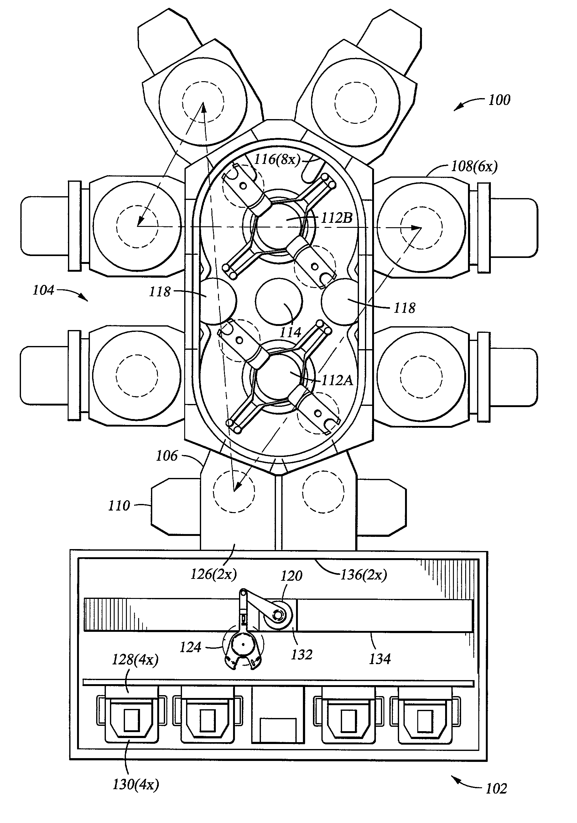
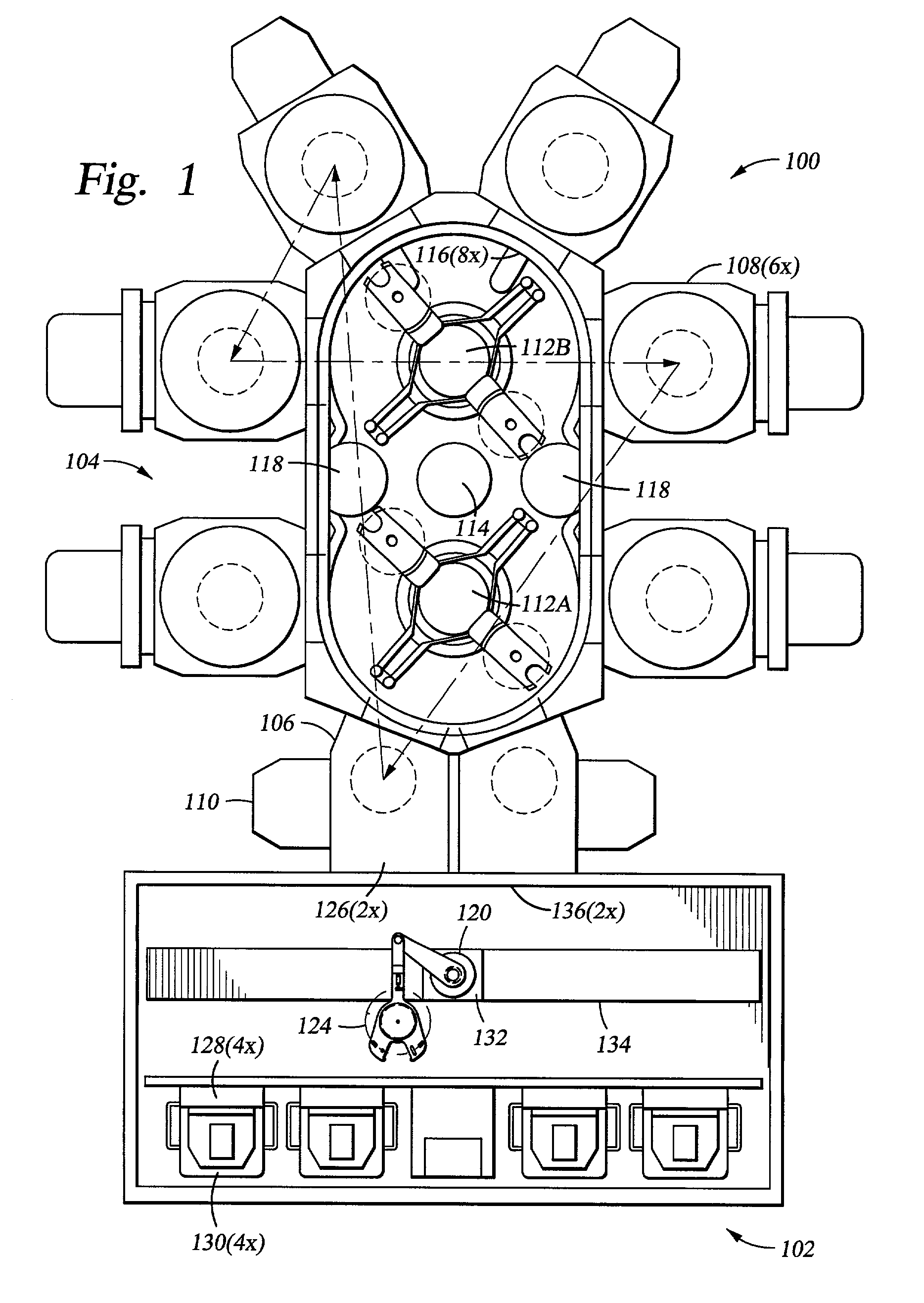
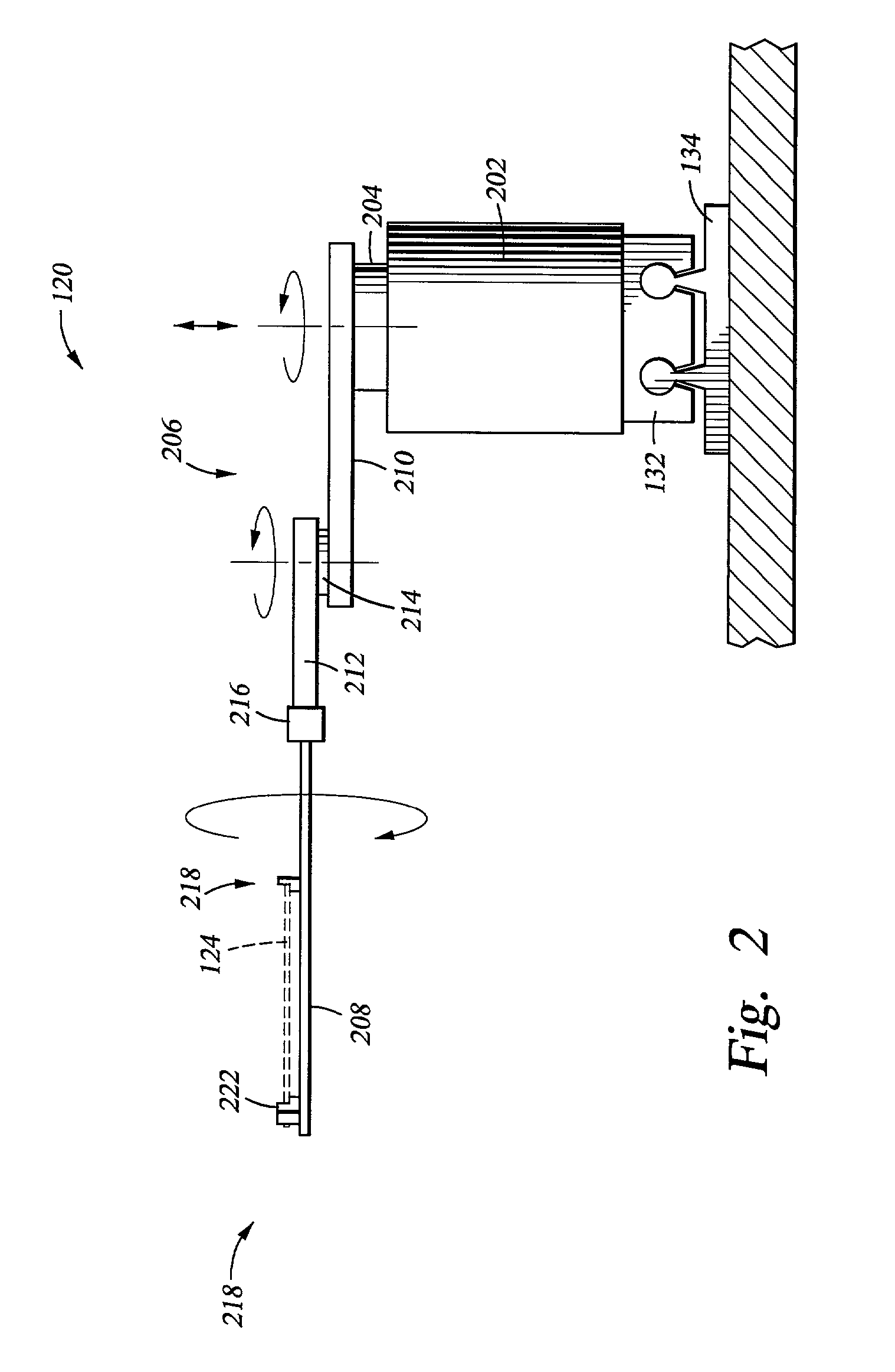
[0024] FIG. 1 depicts a processing system 100 having one embodiment of a substrate transfer mechanism 120 of the present invention disposed therein. The exemplary processing system 100 additionally includes a factory interface 102, a transfer chamber 104, a least one load lock chamber 106 and a plurality of process chambers 108. One example of a processing system that may be adapted to benefit from the invention is an ENDURA.RTM. processing platform, available from Applied Materials, Inc., of Santa Clara, Calif. Although the substrate transfer mechanism 120 is described disposed in the exemplary processing system 100, the description is one of illustration and, accordingly, the substrate transfer mechanism 120 has utility wherever substrate orientation is desired.

[0025] The transfer chamber 104 is generally fabricated from a single piece of material such as aluminum. The chamber 104 defines an evacuable interior 122 through which substrates 124 are transferred between the process ch...


PUM

PropertyMeasurementUnit
timeaaaaaaaaaa
vacuumaaaaaaaaaa
polaraaaaaaaaaa

Abstract

A method and apparatus for transferring a substrate is provided. In one embodiment, an apparatus for transferring a substrate includes at least one end effector. A disk is rotatably coupled to the end effector. The disk is adapted to rotate the substrate relative to the end effector. The end effector may additionally include a sensor coupled thereto. The sensor is adapted to detect an indicia of orientation of the substrate supported by the end effector. In another embodiment, a method for transferring a substrate includes rotating the substrate disposed on an end effector and detecting an indicia of orientation of the substrate.

Description

BACKGROUND OF THE DISCLOSURE[0001] 1. Field of Invention[0002] The embodiments of the present invention generally relate to a method and apparatus for transferring a semiconductor substrate.[0003] 2. Background of Invention[0004] Semiconductor substrate processing is typically performed by subjecting a substrate to a plurality of sequential processes to create devices, conductors and insulators on the substrate. These processes are generally performed in a processing chamber configured to perform a single step of the production process. In order to efficiently complete the entire sequence of processing steps, a number of processing chambers are typically coupled to a central transfer chamber that houses a robot to facilitate transfer of the substrate between the processing chambers. A semiconductor processing platform having this configuration is generally known as a cluster tool, examples of which are the family of CENTURA.RTM. and ENDURA.RTM. processing platforms available from Ap...

Claims


Application Information

Patent Timeline
Patent Type & Authority Applications(United States)
IPC IPC(8): B25J9/06B25J9/10B25J15/08B65G49/07H01L21/677H01L21/68H01L21/687
CPCH01L21/681Y10S414/136Y10S414/141H01L21/68707
Inventor REIMER, PETERPATEL, JAYESH
Owner APPLIED MATERIALS INC
Why Eureka
Try Eureka