Low-noise CMOS Active pixel

a low-noise, active-pixel technology, applied in the field of image sensors, can solve the problems of troublesome reset phase, limited image sensors with cmos active pixels, and inability to adjust the brightness of the image sensor,

Inactive Publication Date: 2003-02-20
STMICROELECTRONICS SRL
View PDF1 Cites 23 Cited by
  • Summary
  • Abstract
  • Description
  • Claims
  • Application Information

AI Technical Summary

Problems solved by technology

At present, the main limitation of image sensors with CMOS active pixels lies in the presence of a reset noise in the electrical signals produced by the pixels of the sensor.
This reset noise is troublesome because it is preponderant over the other noises in the signal-acquisition analog chain.
A first drawback of this pixel structure is that the reset phase gives rise to a reset noise in the photosensitive element.
A power supply noise then gets added to the reset noise in the photodiode.
This phenomenon further reduces the voltage swing of the output signal which is already limited by the generally low value of the power supply voltage and will be increasingly limited, given the current progress of technologies in this field.
Yet still another problem is lag.
This problem appears when a limited bandwidth reset technique is used.
However, this technique reduces reset noise only by a factor of two.
In particular, it entails a large number of transistors (six transistors) per pixel, the need for a high power supply voltage because there are several cascade-mounted transistors, the need for a noise-free voltage ramp, and a mode of implementation which is difficult to render compatible with a matrix of pixels.

Method used


Image

  • Low-noise CMOS Active pixel
  • Low-noise CMOS Active pixel
  • Low-noise CMOS Active pixel

Examples


Embodiment Construction

[0036] It should be understood that these embodiments are only examples of the many advantageous uses of the innovative teachings herein. In general, statements made in the specification of the present application do not necessarily limit any of the various claimed inventions. Moreover, some statements may apply to some inventive features but not to others. In general, unless otherwise indicated, singular elements may be in the plural and vice versa with no loss of generality. In the drawing like numerals refer to like parts through several views.

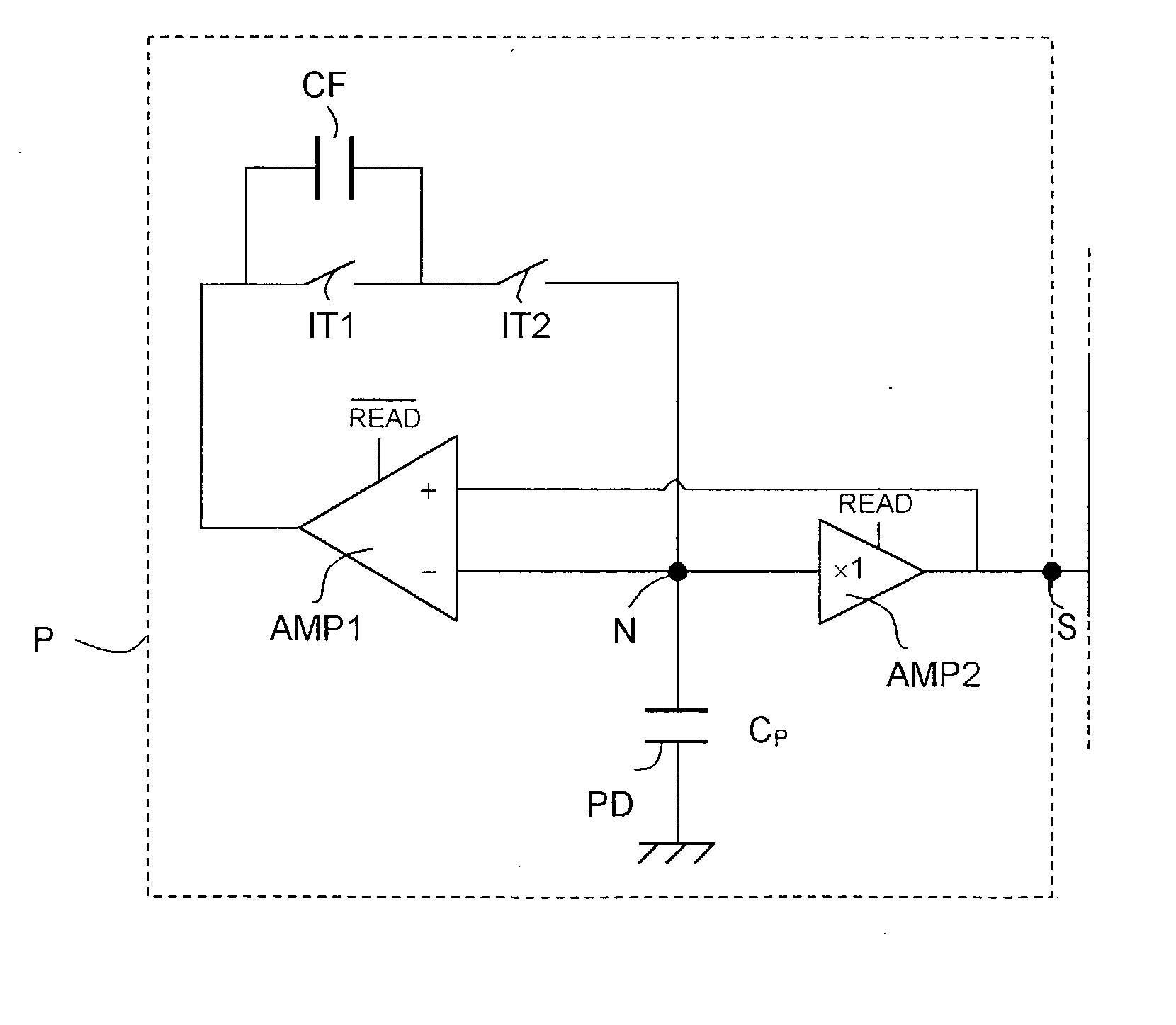
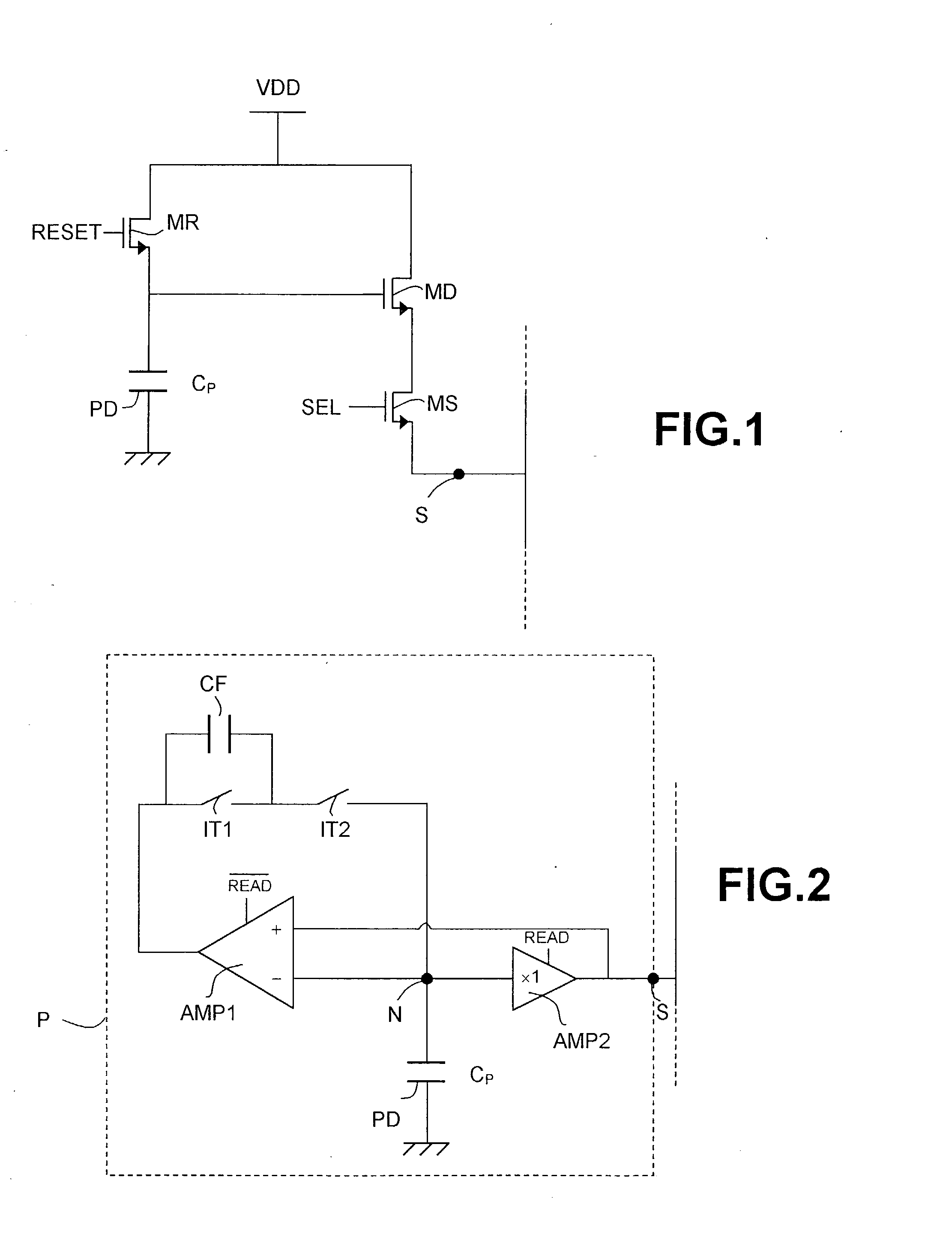
[0037] The general structure of a CMOS active pixel according to the invention is shown in FIG. 2. The CMOS active pixel, referenced P in this FIG., comprises a photodiode PD with a capacitance C.sub.P, an amplifier AMP1 that is active during the reset phase (the signal READ being inactive,) a follower amplifier AMP2 active during the READ phase (with the signal READ active), two switches IT1 and IT2 series-connected between the output and ...


PUM


Abstract

A CMOS active pixel for image sensors has a photosensitive element, a capacitive feedback element with a capacitance CF, and four transistors, namely a first transistor, two reset transistors and a transistor for the selection of the pixel. These transistors are laid out and controlled in such a way that the first transistor is mounted as an amplifier during the pixel reset phase and as a follower during the read phase.

Description

[0001] This application is based upon and claims priority from prior French Patent Application No. 0107349, filed May 28, 2001, the disclosure of which is hereby incorporated by reference in its entirety.[0002] 1. Field of the Invention[0003] The present invention generally relates to the field of image sensors with CMOS active pixels and more particularly to a low-noise CMOS active pixel.[0004] 2. Description of Related Art[0005] At present, the main limitation of image sensors with CMOS active pixels lies in the presence of a reset noise in the electrical signals produced by the pixels of the sensor. This reset noise is troublesome because it is preponderant over the other noises in the signal-acquisition analog chain.[0006] A classic CMOS active pixel essentially comprises a photosensitive element, such as a photodiode, associated with three transistors, a selection transistor to select the pixel, a transistor to reset the electrical charge of the photosensitive element and a rea...

Claims


Application Information

Patent Timeline
Patent Type & Authority Applications(United States)
IPC IPC(8): H01L27/146H04N5/363
CPCH04N5/363H04N25/65
Inventor SIMONY, LAURENT
Owner STMICROELECTRONICS SRL
Why Eureka
Try Eureka