Ceramic shadow-mask in IC process flow

a ceramic and process flow technology, applied in the field of ceramic shadow mask in the ic process flow, can solve the problems of high cost, overlap, and complicated procedures in making a photo mask, and achieve the effect of reducing the complexity and inextricable procedures, and reducing the number of photo masks

Inactive Publication Date: 2003-04-10
MARKETECH INT
View PDF0 Cites 8 Cited by
  • Summary
  • Abstract
  • Description
  • Claims
  • Application Information

AI Technical Summary

Benefits of technology

0007] It is an object of the present invention to lessen the numbers of photomask an

Problems solved by technology

Aforementioned procedures in making a photomask are very complex and overlap and too expensive.
Otherwise, a wafer has various div

Method used


Image

  • Ceramic shadow-mask in IC process flow
  • Ceramic shadow-mask in IC process flow
  • Ceramic shadow-mask in IC process flow

Examples


Embodiment Construction

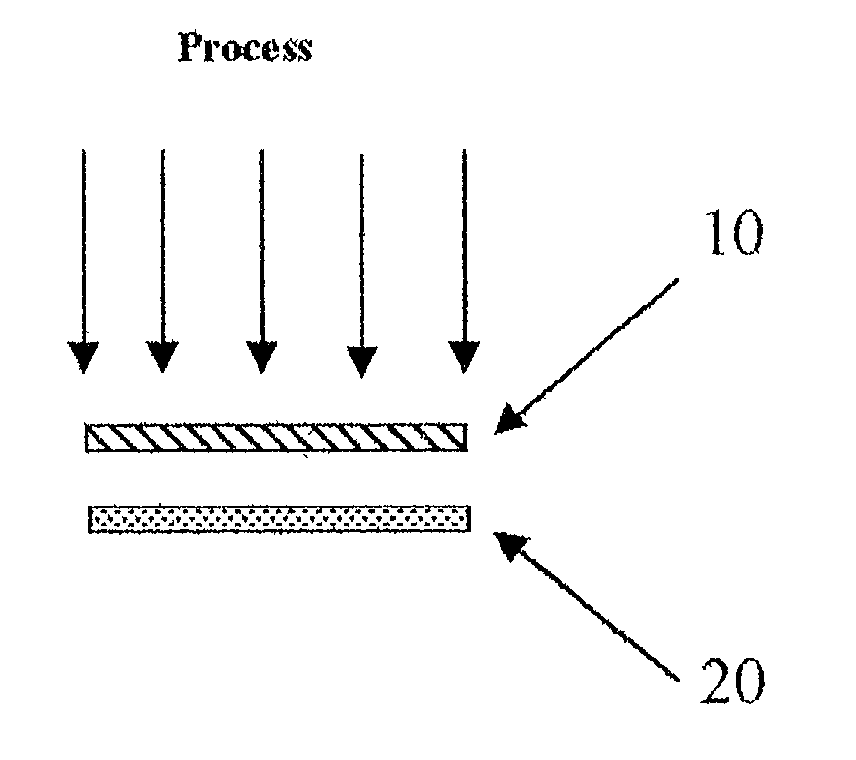
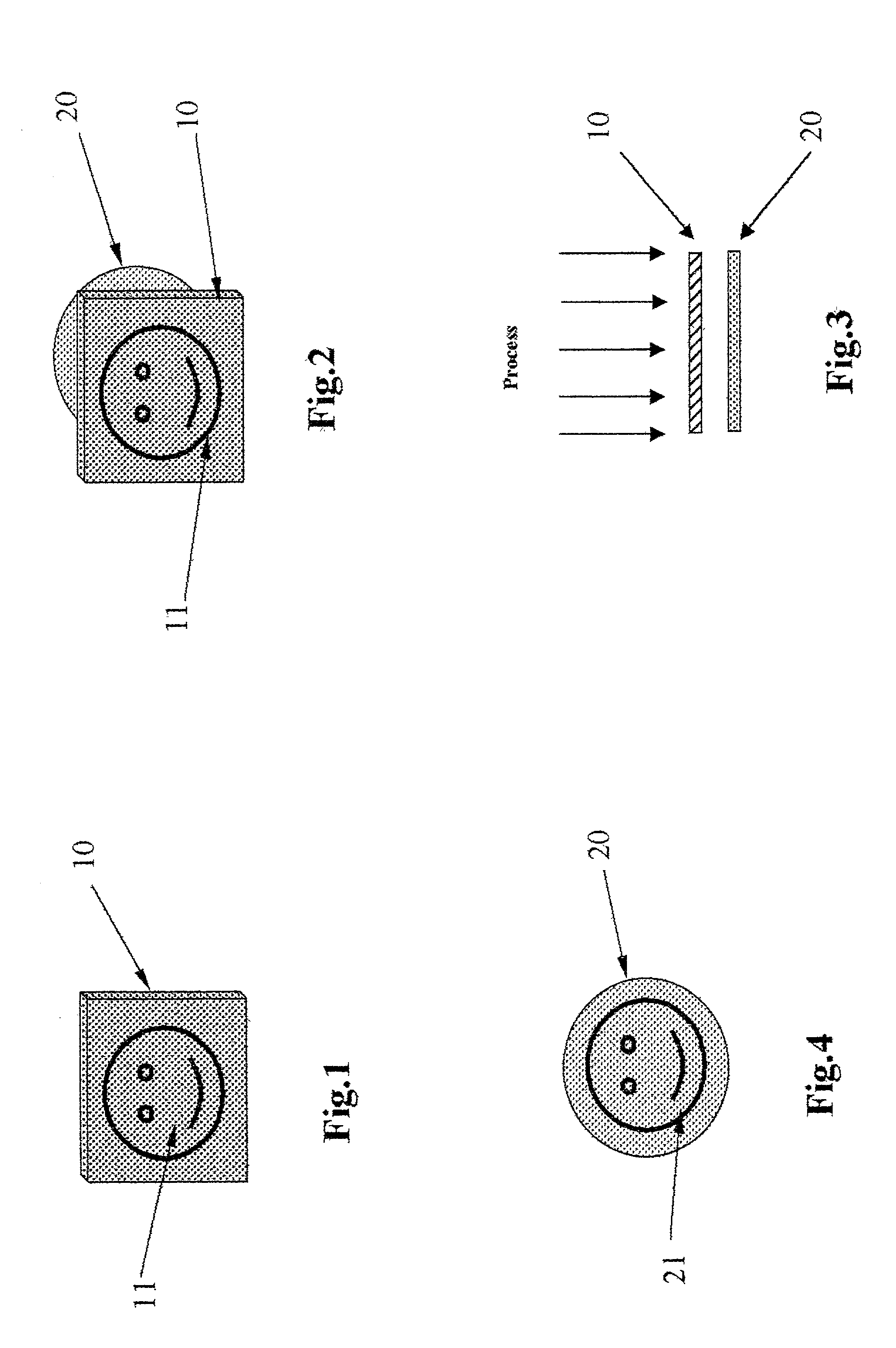
[0025] As defined a ceramic shadow-mask (10) to posses the procedures of photosensitive resist and exposure to form a pattern (11), then by using of wet / dry etching to etch said pattern (11) shown as FIG. 1. Then placed the wafer (20) beneath the etched mask (10) (shown as FIG. 2) and to direct process the procedures of etching, or film growth, or implantation onto both of said mask and wafer (shown as FIG. 3). Since said procedures have been completed, a manufactured wafer (20) is able to take away and the pattern of said mask (11) had been transferred into and printed on the wafer (20) (shown as FIG. 4).

[0026] The ceramic shadow-mask (20) is also capable of processing a partial shadowing, by means of shadowing the division (21) of a partial code which on the upper section of the Wafer (20).

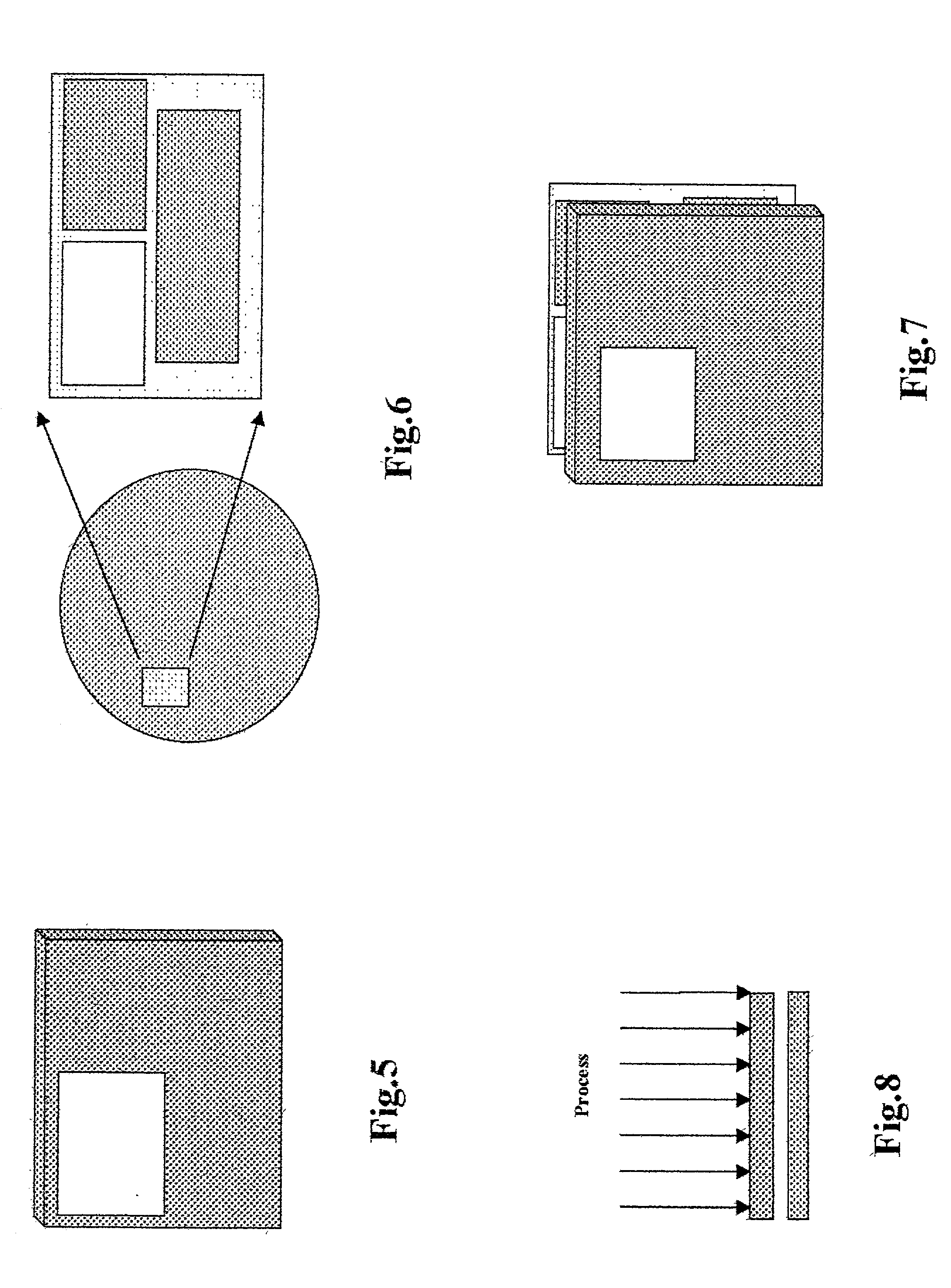
[0027] Please refer to FIGS. 5 from 8, by putting the wafer (20) beneath the ceramic shadow-mask (30) which had been finished the procedures of photosensitive resist, exposure and etching. So th...


PUM


Abstract

The present invention provides a method of ceramic shadow-mask in process flow, which replaces the conventional photomask(s) and applies to the procedures of IC manufacturing to achieve the same efficiency as photomask(s). Additionally, the present invention can combine with photosensitive resist defined pattern to lessen a number of photomask(s) and complex procedures in IC manufacturing, especial in SOC, as well as decrease the cost of mask(s).

Description

[0001] The present invention relates to a method of ceramic shadow-mask in process flow. Namely, by defined a ceramic material for using in the surface of shadow-mask, after exposing the photosensitive resist to form a pattern, then by dry / wet-etching the pattern onto. Since the shadow-mask is been completed, by laying said mask upon a raw wafer to process the etching, film growth and implantation onto said wafer.[0002] Different divisions, e.g. logic and memory divisions, in same chip will need different process requirements on each division. To reach the requirement, the device performance sacrifice or increase mask or apply defined the same ceramic material as aforesaid companying with photosensitive resist defined pattern for partial shadowing and following the aforesaid procedures to process onto said wafer. Stepping by stepping the one shadow mask or more to achieve the one partial shield pattern or more partial shield patterns which is / are according the needs of said wafer. T...

Claims


Application Information

Patent Timeline
IPC IPC(8): H01L21/027
CPCH01L21/027
Inventor LIN, CHIEF
Owner MARKETECH INT
Why Eureka
Try Eureka