Device for testing electrical characteristics of chips

Inactive Publication Date: 2003-05-22
ADVANCED SEMICON ENG INC
View PDF7 Cites 21 Cited by
  • Summary
  • Abstract
  • Description
  • Claims
  • Application Information

AI Technical Summary

Problems solved by technology

For this technology, it is a very important issue about how to increase the stability and reliability of the electrical characteristics of the bumps.
If the bumps have bad connections, the electrical performances and the lifetime of the consumer electronic products will be impacted.
However, the conventional test method often results in many problems, referring to FIGS. 3(a)

Method used


Image

  • Device for testing electrical characteristics of chips
  • Device for testing electrical characteristics of chips
  • Device for testing electrical characteristics of chips

Examples


Embodiment Construction

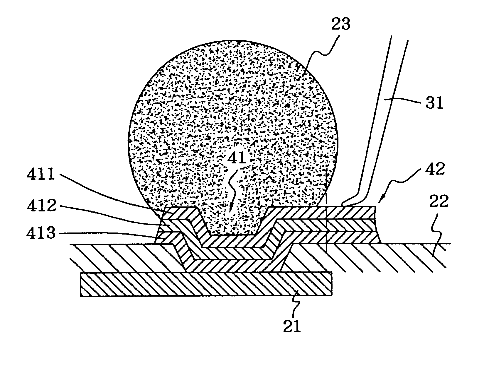
[0020] FIG. 4 is the schematic diagram of the bump bumped on the UBM according to the invention, wherein there is a UBM 41 provided between the bump 23 and the bonding pad 21, which includes an adhesion layer 413, a barrier layer 412 and a wetting layer 411. The UBM 41 is provided with an extension area 42, which laterally extends from the bottommost bump 23. And the area of the extension area 414 is enough for the probe 31 to conduct the test operation, including sufficient contact area for the head of the probe 31 and tolerable area to ensure the probe 31 will not touch the bump 23 while traveling. Furthermore, the extension area 42 is at least formed from one side of the UBM 41, and may be at four sides, which depends on the test requirement. In other words, when the photo mask being designed, it is considered that the extension area 42 covered with photoresist would not be removed during etching process. Because the extension area 42 and the bonding pad 21 are electrically conne...


PUM


Abstract

The present invention discloses a device for testing electrical characteristics of a chip, which is capable of verifying whether each chip can meet the requirement of the electrical specifications, and sort out the chips under the specifications. The invention utilizes a probe to contact the extension area of the under bump metallurgy to detect if the electrical characteristics of the chip can meet the requirement of the specifications. As the bumps on the chip do not actually contact the probe, the intact profile for the bumps on the chips can be assuredly kept so that the problem of voids existing in the melted bumps during reflow process can be avoided.

Description

[0001] 1. Field of the Invention[0002] The present invention relates to a device for testing semiconductor elements, especially to a device for testing electrical characteristics of a chip.[0003] 2. Description of the Related Art[0004] As for the increasing requirement for the portability of consumer electronic products, the flip-chip technology definitely provides the best method to achieve the object of making electrical products lighter, thinner, shorter and smaller. For this technology, it is a very important issue about how to increase the stability and reliability of the electrical characteristics of the bumps. If the bumps have bad connections, the electrical performances and the lifetime of the consumer electronic products will be impacted.[0005] After the completion of the front-end wafer manufacturing process and before the back-end package process, the electrical characteristics of each chip 12 have to be tested on the wafer 11 first, as shown in FIG. 1. If there are defe...

Claims


Application Information

Patent Timeline
IPC IPC(8): G01R31/28H01L23/485
CPCG01R31/2884H01L2224/05554H01L24/03H01L24/05H01L24/11H01L2224/0401H01L2224/05155H01L2224/05564H01L2224/05624H01L2224/05647H01L2224/05666H01L2224/13023H01L2224/131H01L2224/13144H01L2924/01005H01L2924/01006H01L2924/01013H01L2924/01022H01L2924/01028H01L2924/01029H01L2924/0105H01L2924/01079H01L2924/01082H01L2924/014H01L22/32H01L2224/05572H01L2224/05027H01L2924/01033H01L2924/01024H01L2924/01023H01L2924/00014H01L2224/0392
Inventor FANG, JEN-KUANG
Owner ADVANCED SEMICON ENG INC
Why Eureka
Try Eureka