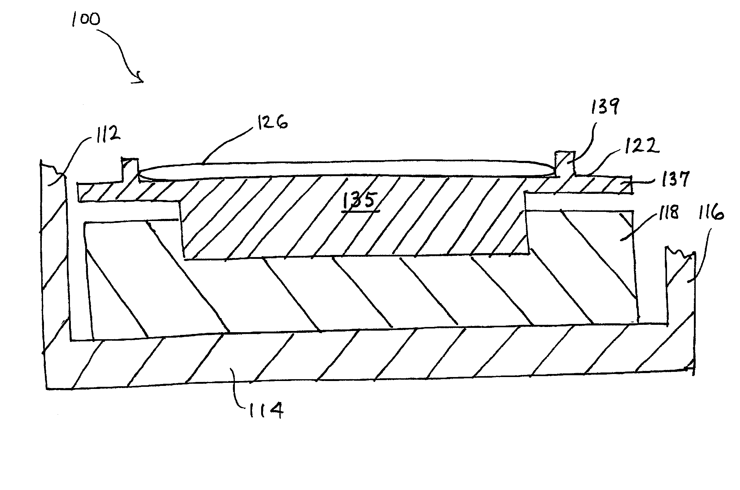
Wafer carrier for semiconductor process tool
a technology of process tools and wafers, applied in the field of wafers, can solve the problems of time-consuming and costly, time-consuming in such reconfiguration,
- Summary
- Abstract
- Description
- Claims
- Application Information
AI Technical Summary
Benefits of technology
Problems solved by technology
Method used
Image

Examples
example
[0084] A wafer carrier was constructed of the general type shown in FIGS. 1 and 2 hereof. The wafer carrier was constructed of silicon carbide with a recess of 100 mm diameter therein. The overall wafer carrier diameter was 150 mm. The edges of the wafer were thinned to allow the wafer to readily fit into the slots of a wafer carrier cassette.
[0085] Mechanical tests were conducted and the wafer carrier and 100 mm wafer were successfully transferred into and subsequently removed from the growth chamber of the epitaxial reactor (Centura reactor, commercially available from Applied Materials, Inc.).
[0086] A comparative test was then conducted of epitaxial thin film growth on wafers of 100 mm diameter and 150 mm diameter, in which the 150 mm diameter wafer was directly inserted into a correspondingly sized and shaped recess in the susceptor of the reactor, and in which the 100 mm diameter wafer was processed in a 150 mm diameter wafer carrier which in turn was inserted into the recess i...
PUM
 Abstract
Description
Claims
Application Information