

Method and system for optical proximity correction
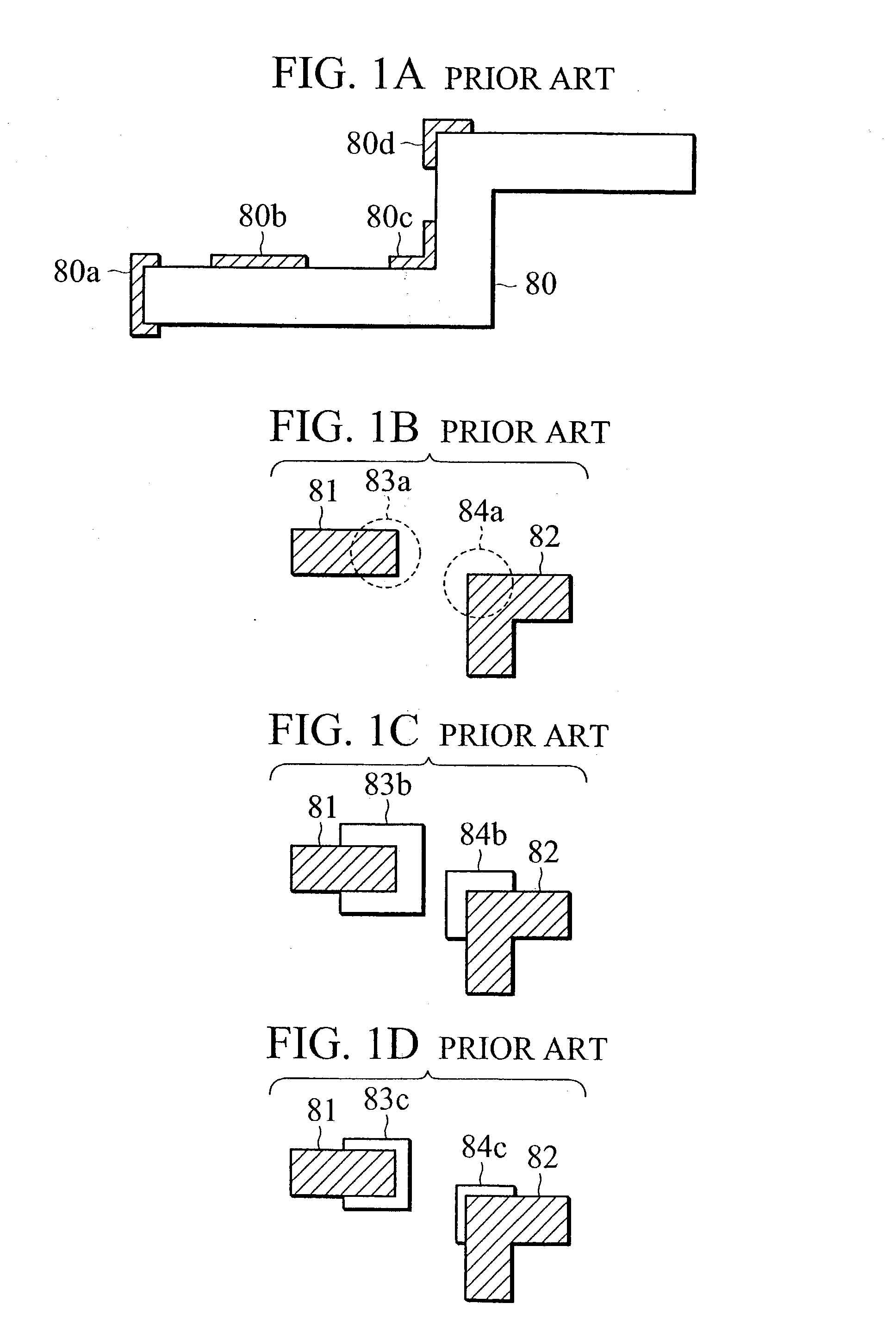
a technology of optical proximity and correction method, applied in the field of optical proximity correction method and system, can solve the problems of increasing the number of patterns that cannot be corrected properly, opc fails to solve, and it is difficult to generate precise minute mask patterns on a wafer through optical exposur
- Summary
- Abstract
- Description
- Claims
- Application Information
AI Technical Summary
Problems solved by technology
Method used
Image

Examples
Embodiment Construction
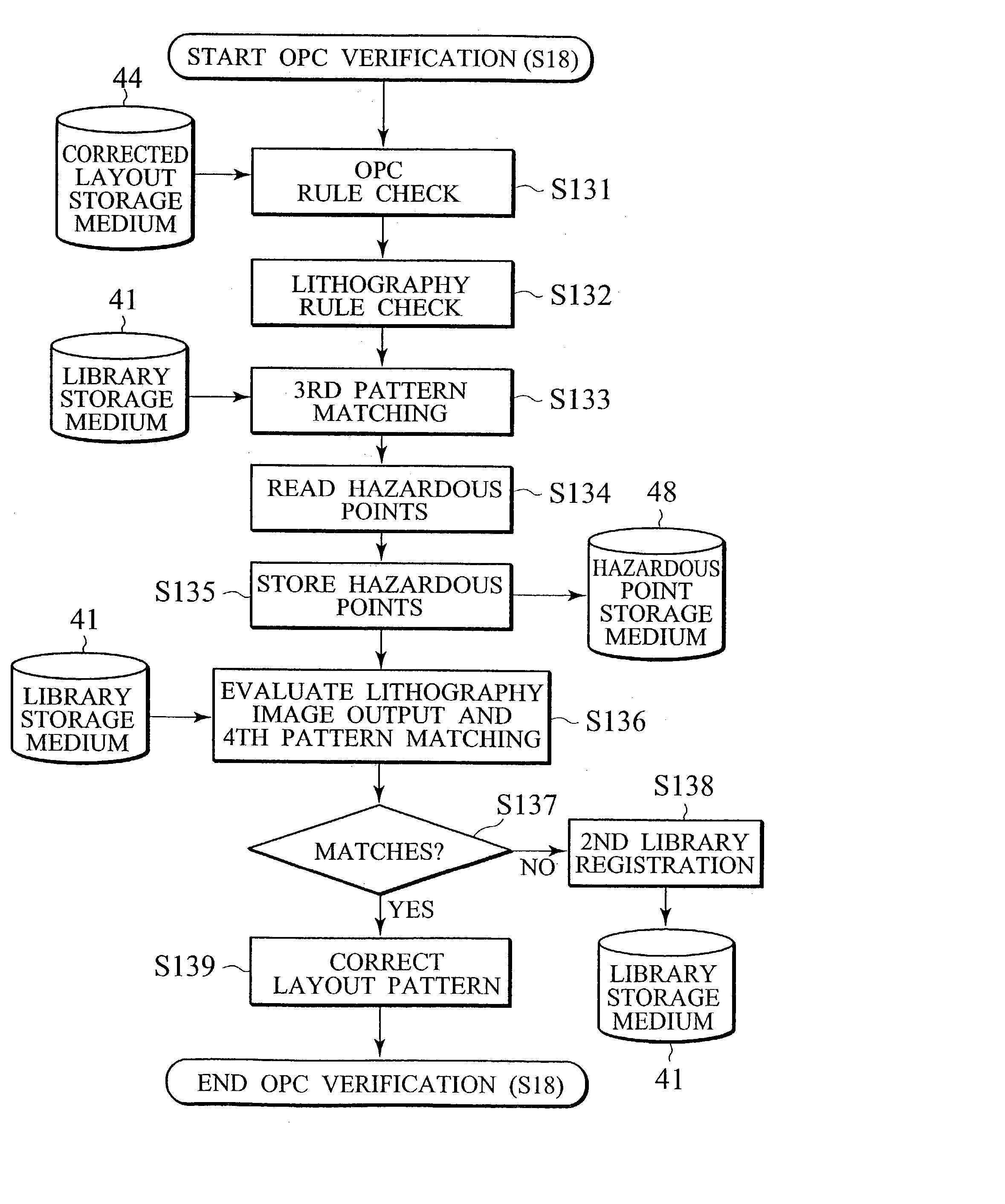
[0053] Various embodiments of the present invention will be described with reference to the accompanying drawings. It is to be noted that the same or similar reference numerals are applied to the same or similar parts and elements throughout the drawings, and the description of the same or similar parts and elements will be omitted or simplified.
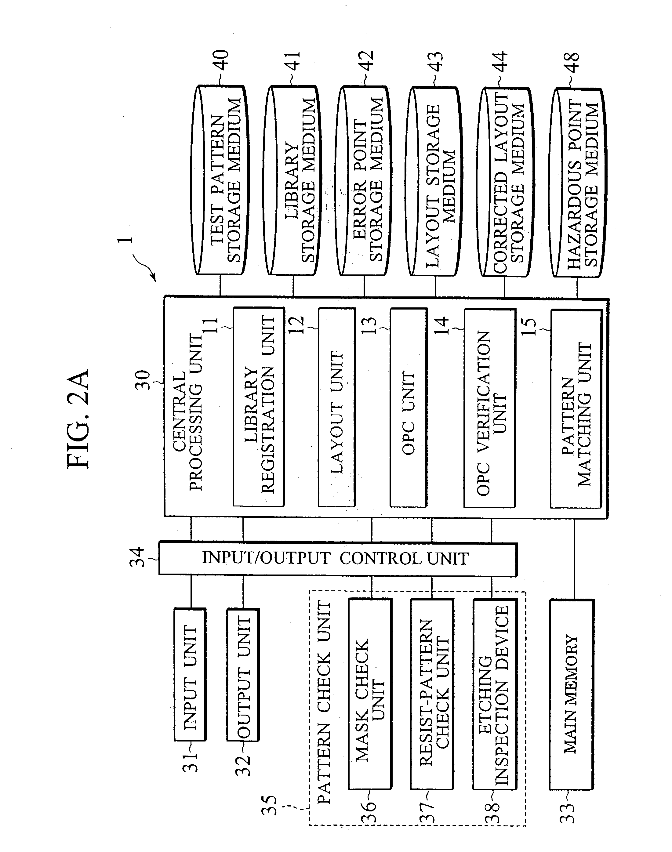
[0054] In the following descriptions, numerous specific details are set fourth such as specific signal values, etc. to provide a thorough understanding of the present invention. However, it will be obvious to those skilled in the art that the present invention may be practiced without such specific details in other instances, well-known circuits have been shown in block diagram generate in order not to obscure the present invention in unnecessary detail. In the following description of the embodiments, an optical proximity correction (OPC) system, which can speed up the OPC process to verify the validity of the post-OPC pattern, and an OPC m...
PUM
 Abstract
Description
Claims
Application Information