

Semiconductor laser device including arrow structure precisely formed to suppress P-As interdiffusion and Al oxidation
a laser device and semiconductor technology, applied in the direction of lasers, lasers, semiconductor lasers, etc., can solve the problems of inability to achieve the above semiconductor laser element, regrowth is likely to be defective, and the optical density in the active layer increases
- Summary
- Abstract
- Description
- Claims
- Application Information
AI Technical Summary
Benefits of technology
Problems solved by technology
Method used
Image

Examples
first embodiment
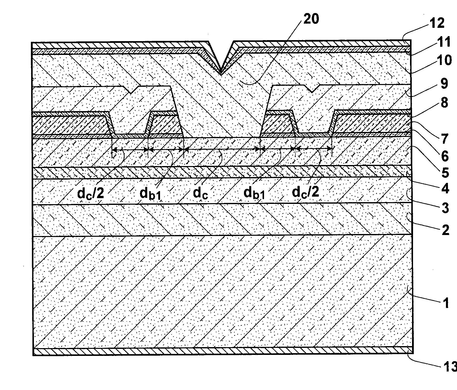
[0059] The semiconductor laser element as the first embodiment of the present invention is explained below. FIG. 1 is a cross-sectional view of the semiconductor laser element as the first embodiment.
[0060] As illustrated in FIG. 1, the semiconductor laser element as the first embodiment comprises a stack of an n-type Al.sub.z1Ga.sub.1-z1As lower cladding layer 2 (0.2.ltoreq.z1.ltoreq.0.8), an n-type or i-type (intrinsic) GaAs lower optical waveguide layer 3, an In.sub.x3Ga.sub.1-x3As.sub.1-y3P.sub.y3 quantum-well active layer 4 (0.49y3<x3.ltoreq.0.4, 0.ltoreq.y3.ltoreq.0.1), and a p-type or i-type GaAs upper optical waveguide layer 5 which are formed on an n-type GaAs substrate 1. In addition, a p-type In.sub.x8Ga.sub.1-x8P first etching stop layer 6 (0.ltoreq.x8.ltoreq.1), an n-type GaAs first current confinement layer 7, a p-type In.sub.x9Ga.sub.1-x9P second etching stop layer 8 (0.ltoreq.x9.ltoreq.1) , an n-type Al.sub.z1Ga.sub.1-z1As second current confinement layer 9, a p-type...
second embodiment
[0068] The semiconductor laser element as the second embodiment of the present invention is explained below. FIG. 3 is a cross-sectional view of the semiconductor laser element as the second embodiment. The elements in FIG. 3 which bear the same reference numerals as FIG. 1 have the same functions as the corresponding elements in FIG. 1. Therefore, the explanations on those elements are not repeated here.
[0069] As illustrated in FIG. 3, the semiconductor laser element as the second embodiment is different from the semiconductor laser element as the first embodiment in that an InGaAs quantum-well layer 14 is formed at a mid-thickness of the n-type GaAs first current confinement layer 7, where the InGaAs quantum-well layer 14 has a bandgap smaller than the i-type In.sub.x3Ga.sub.1-x3As.sub.1-y3P.sub.y3 quantum-well active layer 4. Since the InGaAs quantum-well layer 14 absorbs light, the gain in the fundamental transverse mode can be increased when the semiconductor laser element comp...
third embodiment
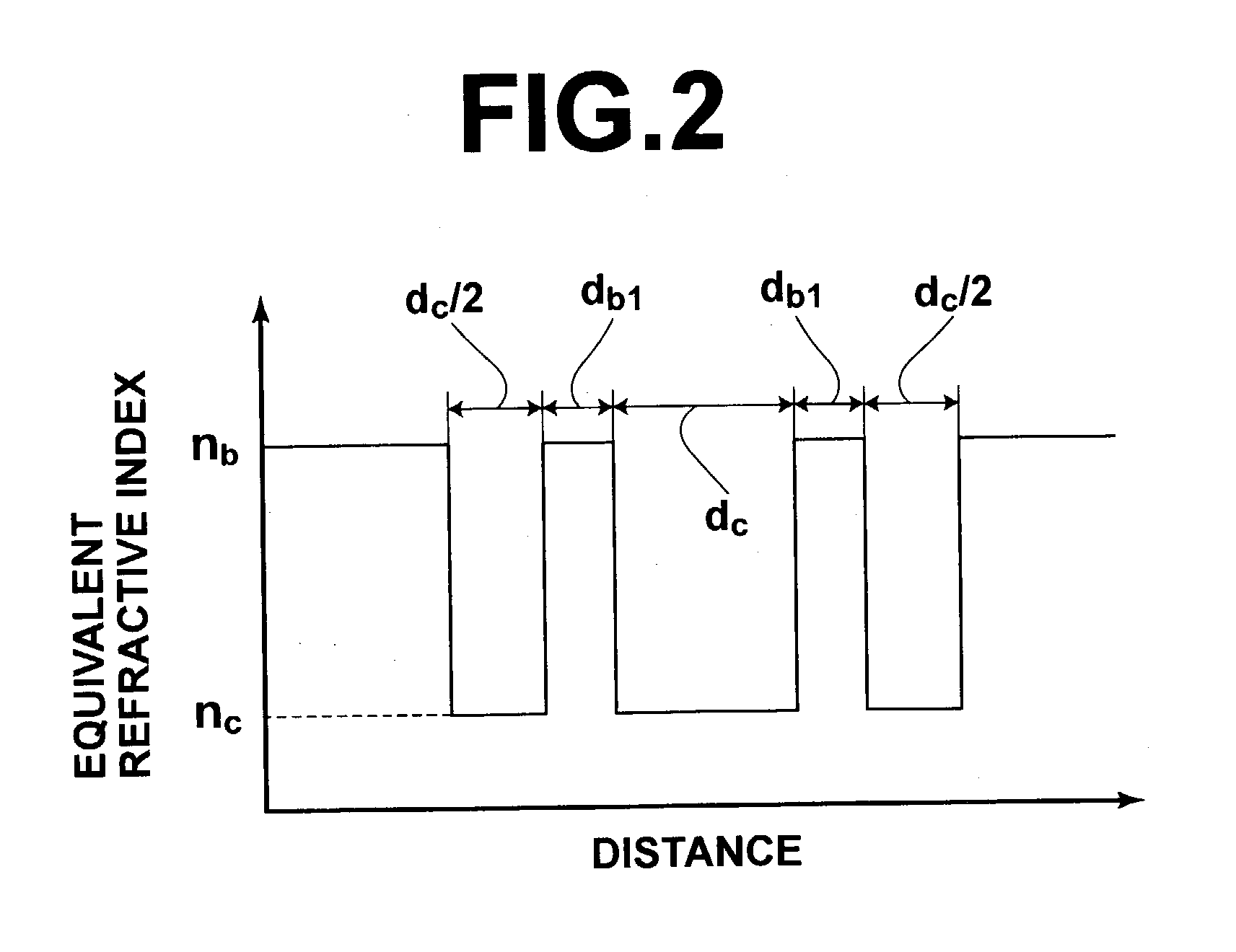
[0074] Although the semiconductor laser devices as the first and second embodiments of the present invention has a single-core ARROW structure, it is possible to form a multicore ARROW structure having a plurality of core regions. In this case, for example, a distribution of the equivalent refractive index of an active layer in the direction perpendicular to thickness and propagation of light is realized as illustrated in FIG. 5.
[0075] FIG. 5 shows a distribution of the equivalent refractive index of the active layer in the direction perpendicular to thickness and propagation of light in a semiconductor laser device having a multicore ARROW structure. In the distribution illustrated in FIG. 5, the plurality of core regions have a low equivalent refractive index n.sub.c, outermost ones of a plurality of high-refractive-index stripe regions having a high equivalent refractive index n.sub.b each have a width d.sub.b1, and the other high-refractive-index stripe regions having the high e...
PUM
 Abstract
Description
Claims
Application Information