Check patentability & draft patents in minutes with Patsnap Eureka AI!

Stripe type semiconductor light emitting element having InGan active layer, combined with optical resonator including wavelength selection element

a technology of ingan active layer and wavelength selection element, which is applied in the direction of lasers, optical resonator shape and construction, and semiconductor laser devices emitted green and blue laser beams that are not practicable at present, and can solve the problems of inability to achieve the effect of reducing the volume of light emission, prone to variation of wavelength of emitted light, and inability to achieve the effect of reducing the amount of light emission

Inactive Publication Date: 2003-08-07
NICHIA CORP
View PDF3 Cites 15 Cited by
  • Summary
  • Abstract
  • Description
  • Claims
  • Application Information

AI Technical Summary

Benefits of technology

The solution effectively suppresses wavelength and intensity variations, enabling the semiconductor light emitting apparatus to produce stable green or blue light with small beam diameter and divergence angle, suitable for color image printing and other applications.

Problems solved by technology

Nevertheless, semiconductor laser devices emitting green and blue laser beams are not practically available at present.
However, the conventional semiconductor light emitting devices have a drawback that the wavelength of emitted light is prone to vary due to characteristics of the InGaN material, as explained below.
Nevertheless, since light emission occurs in the local area in this case, the volume contributing to the light emission is limited.
The above variation in the wavelength of the light emitted from the InGaN active layer is seriously disadvantageous to the aforementioned optical-scanning color image printing apparatuses.
Therefore, such a semiconductor light emitting apparatus cannot be used in the aforementioned optical-scanning color image printing apparatuses due to the variation of the intensity.

Method used


Image

  • Stripe type semiconductor light emitting element having InGan active layer, combined with optical resonator including wavelength selection element
  • Stripe type semiconductor light emitting element having InGan active layer, combined with optical resonator including wavelength selection element
  • Stripe type semiconductor light emitting element having InGan active layer, combined with optical resonator including wavelength selection element

Examples


first embodiment

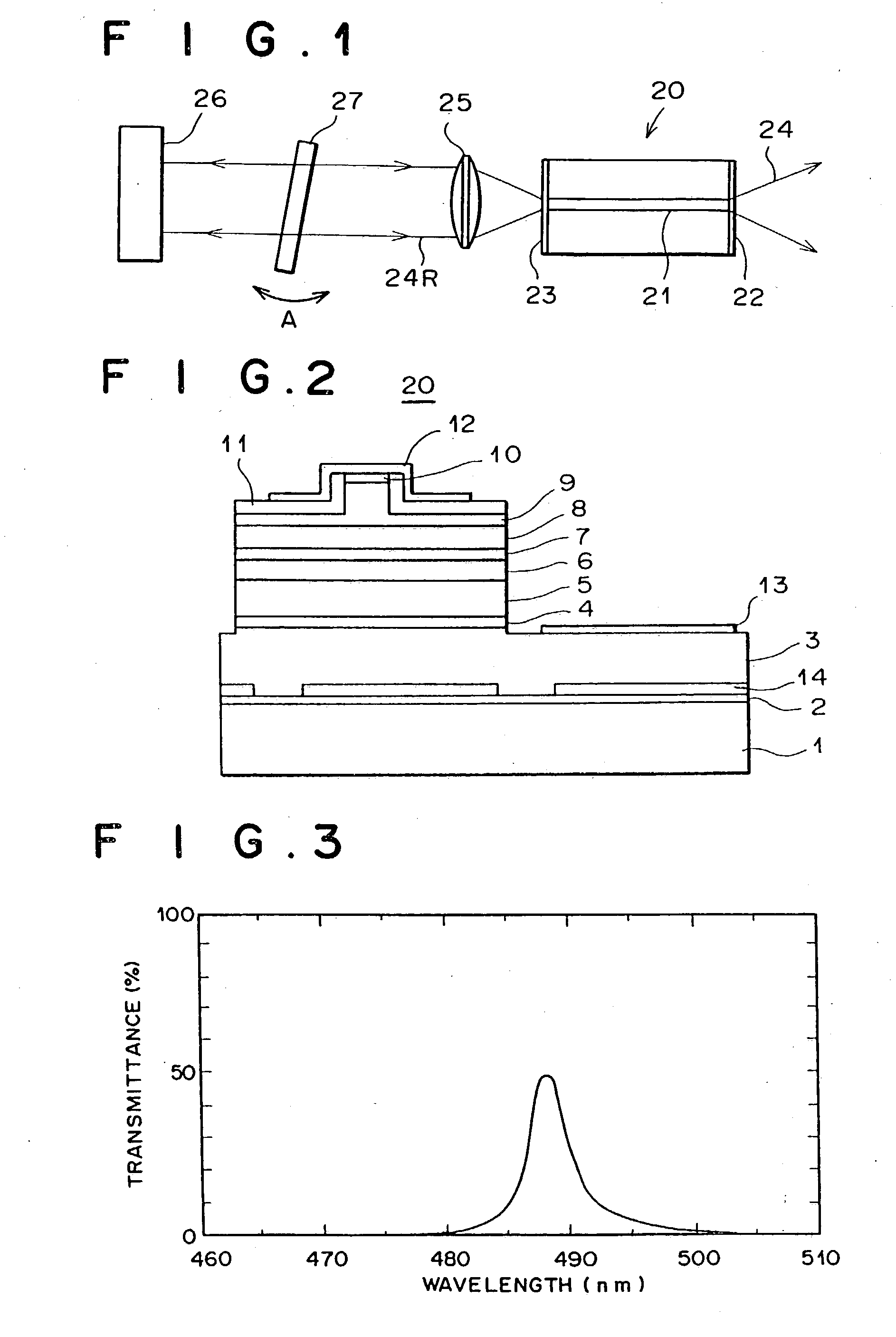
[0054] FIG. 1 is a plan view illustrating an outline of the construction of the semiconductor light emitting apparatus as the first embodiment of the present invention, and FIG. 2 is a cross-sectional view illustrating a longitudinal section of a semiconductor light emitting element 20 used in the construction of FIG. 1.

[0055] First, the semiconductor light emitting element 20 is explained below with reference to FIG. 2.

[0056] The semiconductor light emitting element 20 includes a double heterostructure in which an active layer 7 is sandwiched by cladding layers 5 and 9, a current injection window having a stripe-like shape is provided in a cap layer 10 for confining light, and an optical reflection structure is realized by cleavage planes (as reflection surfaces) of the semiconductor light emitting element.

[0057] The construction of the semiconductor light emitting element 20 and a method for producing the semiconductor light emitting element 20 are explained in detail below.

[0058]...

second embodiment

[0070] FIG. 4 is a plan view illustrating an outline of the construction of the semiconductor light emitting apparatus as the second embodiment of the present invention. In FIG. 4, elements having the same reference numbers as FIG. 1 have the same functions as the corresponding elements in FIG. 1.

[0071] In the semiconductor light emitting apparatus of FIG. 4, a collimator lens 25 and a reflective-type bulk grating element 30 are arranged on the backward side of the semiconductor light emitting element 20. The collimator lens 25 collimates backward light 24R output from the semiconductor light emitting element 20. The reflective-type bulk grating element 30 reflects the collimated backward light 24R to feed it back to the semiconductor light emitting element 20. In the construction of FIG. 4, an external resonator is realized by the bulk grating element 30 and the forward end surface of the semiconductor light emitting element 20. The bulk grating element 30 realizes a wavelength sel...

third embodiment

[0072] FIG. 5 is a plan view illustrating an outline of the construction of the semiconductor light emitting apparatus as the third embodiment of the present invention. In FIG. 5, elements having the same reference numbers as FIG. 1 have the same functions as the corresponding elements in FIG. 1.

[0073] In the semiconductor light emitting apparatus of FIG. 5, a collimator lens 25, a condenser lens 40, and a fiber Bragg grating 41 are arranged on the backward side of the semiconductor light emitting element 20. The collimator lens 25 collimates backward light 24R output from the semiconductor light emitting element 20. The condenser lens 40 collects the collimated backward light 24R.

[0074] The fiber Bragg grating 41 is an optical fiber including a core which is embedded in cladding and has a higher refractive index than the cladding. In the core, a plurality of index varied portions are formed at regular intervals. The backward light 24R collected by the condenser lens 40 converges at...


PUM


Abstract

A semiconductor light emitting apparatus includes a semiconductor light emitting element which includes a stripe structure and an active layer made of an InGaN material, and emits first light without laser oscillation; an optical resonator; and a first wavelength selection unit which allows resonance, in the optical resonator, of second light having a selected wavelength included in the first light emitted by the semiconductor light emitting element. Alternatively, instead of the first wavelength selection unit, a second wavelength selection unit which allows output of only the above second light from the semiconductor light emitting apparatus may be provided. In this case, the semiconductor light emitting apparatus may further include an optical detector which detects intensity of the second light; and an output regularizing unit which drives the semiconductor light emitting element based on the detected intensity so as to regularize the intensity of the second light.

Description

[0001] 1. Field of the Invention[0002] The present invention relates to a semiconductor light emitting apparatus using a semiconductor light emitting element which has an active layer made of an InGaN material and stripe structure, and in which laser oscillation does not occur.[0003] 2. Description of the Related Art[0004] Conventionally, various optical-scanning color image printing apparatuses have been provided. Such apparatuses scan a sheet of color sensitive material with three color recording light beams so as to expose the sheet of color sensitive material to the three color recording light beams, and record a color image in the sheet of color sensitive material. These optical-scanning color image printing apparatuses can be broadly classified into two types. In the first type, the three color recording light beams are red, green, and blue light beams, and the usual color sensitive materials for exposure with visible light are used. In the second type, the above three color r...

Claims


Application Information

Patent Timeline
Patent Type & Authority Applications(United States)
IPC IPC(8): H01L33/00H01L33/20H01L33/32H01L33/48H01S5/0683H01S5/10H01S5/14H01S5/223H01S5/343
CPCB82Y20/00H01L33/0045H01S5/0683H01S5/34333H01S5/141H01S5/2231H01S5/1078Y02E10/50
Inventor HAYAKAWA, TOSHIRO
Owner NICHIA CORP
Features
  • R&D
  • Intellectual Property
  • Life Sciences
  • Materials
  • Tech Scout
  • Unparalleled Data Quality
  • Higher Quality Content
  • 60% Fewer Hallucinations
Learn More