Method of metal electro-plating for IC package substrate

a technology of metal electroplating and ic package, which is applied in the direction of printed element electric connection formation, non-metallic protective coating application, and semiconductor/solid-state device details. it can solve the problem of noise generation affecting the integrity of the signal

Inactive Publication Date: 2003-09-04
ORIENT SEMICON ELECTRONICS
View PDF0 Cites 14 Cited by
  • Summary
  • Abstract
  • Description
  • Claims
  • Application Information

AI Technical Summary

Problems solved by technology

In addition, noise will be generated to affect the integrity of signal.

Method used


Image

  • Method of metal electro-plating for IC package substrate
  • Method of metal electro-plating for IC package substrate
  • Method of metal electro-plating for IC package substrate

Examples


Embodiment Construction

[0014] The following descriptions are of exemplary embodiments only, and are not intended to limit the scope, applicability or configuration of the invention in any way. Rather, the following description provides a convenient illustration for implementing exemplary embodiments of the invention. Various changes to the described embodiments may be made in the function and arrangement of the elements described without departing from the scope of the invention as set forth in the appended claims.

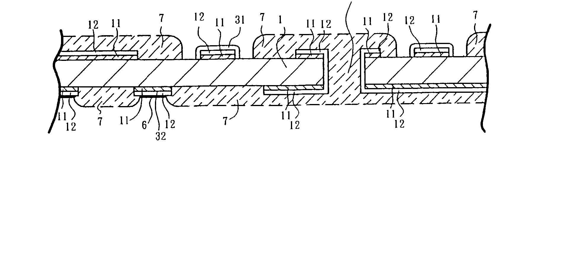
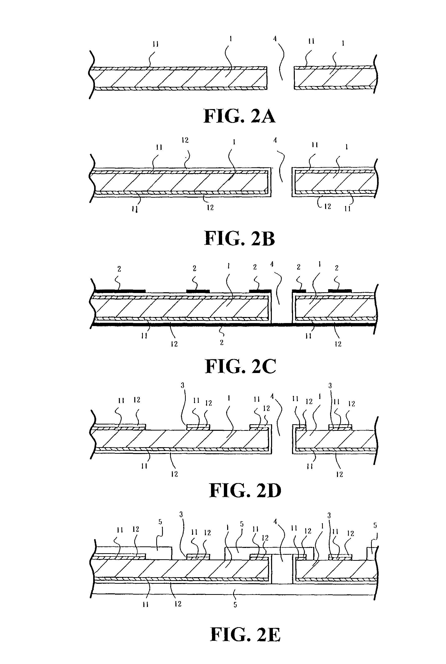
[0015] Referring to FIG. 2, the method of metal electro-plating for IC package substrate. In accordance with the present invention, the method of metal electro-plating for IC package substrate comprises the steps of:

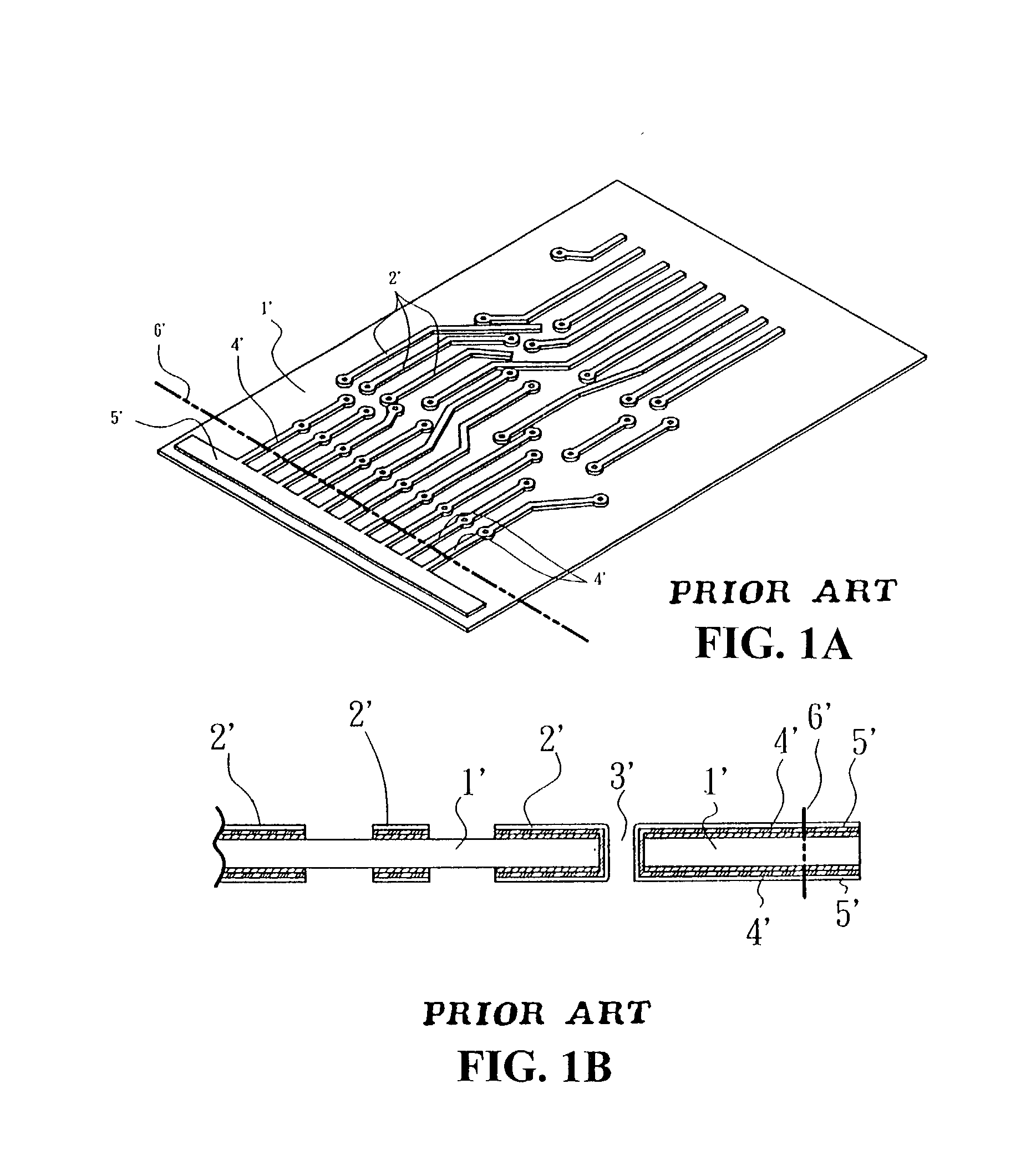
[0016] (a) forming vias 4 on the package substrate 1 coated with copper film 11 on both sides thereof (shown as FIG. 2A);

[0017] (b) electro-plating the vias 4 to form electrical conductive holes between the top layer and the bottom layer of the package substrate 1 (referring to FIG. ...


PUM

PropertyMeasurementUnit
electrical conductiveaaaaaaaaaa

Abstract

A method of metal-electro-plating for IC package substrate comprising the steps of: forming vias on the package substrate coated with copper film on both sides thereof; electro-plating the vias to form electrical conductive holes between the top layer and the bottom layer of the package substrate; coating a resisting agent where the patterns should be formed on the top layer and on the entire bottom layer of the package substrate; etching the pattern to form circuit without plating lines on the top layer of the substrate, and removing the resisting agent; coating with a resisting agent on the top side and the bottom side of the package substrate but the wiring position to be electro-plated as surface finish for wire-bonding electro-plating on the top side of the package substrate not being applied with the resisting agent; electro-plating the substrate with nickel and gold, and removing the resisting agent; fabricating the circuit on the bottom side of the package substrate and coating with a resisting agent to cover the entire top side and where the circuit is to be formed on the bottom side; etching the substrate to obtain the circuit on the bottom side of the package substrate; and coating solder resist on the region other than the circuit section and applying pre-flux onto the circuit section to form into a protective film.

Description

[0001] (a) Technical Field of the Invention[0002] The present invention relates to a metal electro-plating for IC package substrate, and in particular, to a method of electro-plating metal to form a circuit.[0003] (b) Description of the Prior Art[0004] FIGS. 1A and 1B show a conventional dual surface package substrate where the circuits on each layer are connected with plated through holes. The electro-plating method of the substrate is normally the conventional type where at an appropriate position, an electro-plating lead is extended to the plating bar and is then cut off upon completion. At this instance plating tails remain on the substrate and such residues will generate heat while working. In addition, noise will be generated to affect the integrity of signal.[0005] Accordingly, a main object of the present invention is to provide a method of metal electro-plating for IC package substrate, which overcomes the above-mentioned drawbacks.[0006] The present invention relates to a ...

Claims


Application Information

Patent Timeline
Patent Type & Authority Applications(United States)
IPC IPC(8): C25D7/00C25D5/02H01L23/12H05K3/06H05K3/24H05K3/28H05K3/42
CPCH05K3/064H05K3/243H05K2203/1476H05K3/427H05K2201/0352H05K3/282
Inventor HUANG, FU-YUHUANG, YU-CHUNCHUANG, CHIN-HUITSENG, YA-SHINCHIANG, CHI-JUHUNG, PEI-FENLEE, WEI-YINLO, SHU-HUICHEN, CHE-CHEN
Owner ORIENT SEMICON ELECTRONICS
Why Eureka
Try Eureka