Spin valve sensor with exchange biased free layer and antiparallel (AP) pinned layer pinned without a pinning layer

a technology of anti-parallax and free layer, which is applied in the field of spin valve sensor with exchange biased free layer and anti-parallax (ap) pinned layer pinned without a pinning layer, can solve the problems of unwanted extraneous fields, corrosive materials, and difficult schemes

Inactive Publication Date: 2003-09-25
IBM CORP
View PDF10 Cites 40 Cited by
  • Summary
  • Abstract
  • Description
  • Claims
  • Application Information

AI Technical Summary

Benefits of technology

[0017] The present invention employs cobalt iron (CoFe) for each of the first and second AP pinned layers in a self-pinned AP pinned layer structure, however, the iron (Fe) content in the cobalt iron (CoFe) in the first and second AP pinned layers is different for improving the magnetostriction uniaxial anisotropy field while maintaining a high magnetoresistive coefficient dr / R. More specifically, the iron (Fe) content in the cobalt iron (CoFe) of one of the first and second AP pinned layers is greater than the iron (Fe) content in the cobalt iron (CoFe) in the other of the first and second AP pinned layers. In one embodiment of the invention the iron (Fe) content in the cobalt iron (CoFe) in the first AP pinned layer, which does not interface the spacer layer, is greater than the iron (Fe) content in the cobalt iron (CoFe) in the second AP pinned layer which interfaces the spacer layer. Experiments, which are explained in the aforementioned co-pending application, show that when the content of the first AP pinned layer comprises Co.sub.60Fe.sub.40 and the content of the second AP pinned layer comprises Co.sub.90Fe.sub.10 amplitude output and magnetostriction uniaxial anisotropy field are significantly improved while maintaining a high magnetoresistive coefficient dr / R.

Problems solved by technology

If the self-pinning of the AP pinned layer structure is not sufficient, unwanted extraneous fields can disturb the orientations of the magnetic moments of the AP pinned layers or, in a worst situation, could reverse their directions.
While the blocking temperatures of other AFM materials, such as iron manganese (FeMn) and iridium manganese (IrMn), are lower, each of these materials is corrosive.
This scheme is very challenging, especially for very narrow track widths.
Unfortunately, the magnetic field through the free layer between the first and second side surfaces is not uniform since a portion of the magnetization is lost in a central region of the free layer to the shield layers.
If the pinning layer is reset, as described hereinabove, a subsequent reset of the biasing layer would disturb the resetting of the pinning layer.
Alternatively, if platinum manganese is employed for the pinning layer and another AFM material is employed for the biasing layers with a lower blocking temperature, two problems accrue.
The first problem is that there is no suitable AFM material, other than platinum manganese, for pinning or biasing layers because of the corrosion problem and secondly, even though the setting of the biasing layers is at a temperature lower than the blocking temperature of platinum manganese, the magnetic spins of the platinum manganese pinning layer are still disturbed to some extent which lowers the exchange coupling between the pinning layer in the AP pinned layer structure.
Unfortunately, the first and second hard bias layers 140 and 144 in FIG. 9 do not uniformly stabilize a free layer within the sensor 74.
With submicron track widths, this loss in width at each end of the sensor is unacceptable.

Method used


Image

  • Spin valve sensor with exchange biased free layer and antiparallel (AP) pinned layer pinned without a pinning layer
  • Spin valve sensor with exchange biased free layer and antiparallel (AP) pinned layer pinned without a pinning layer
  • Spin valve sensor with exchange biased free layer and antiparallel (AP) pinned layer pinned without a pinning layer

Examples


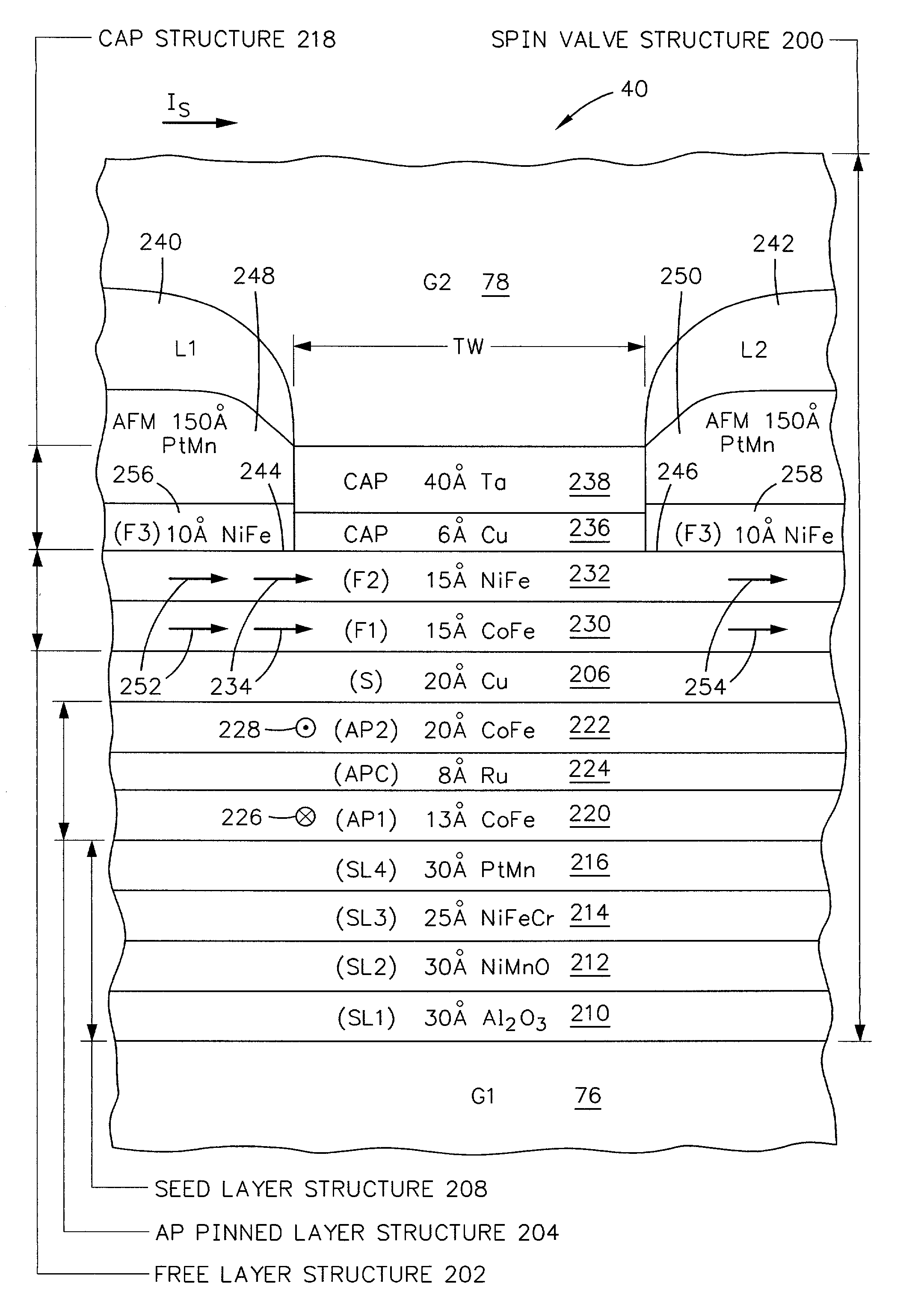
Embodiment Construction

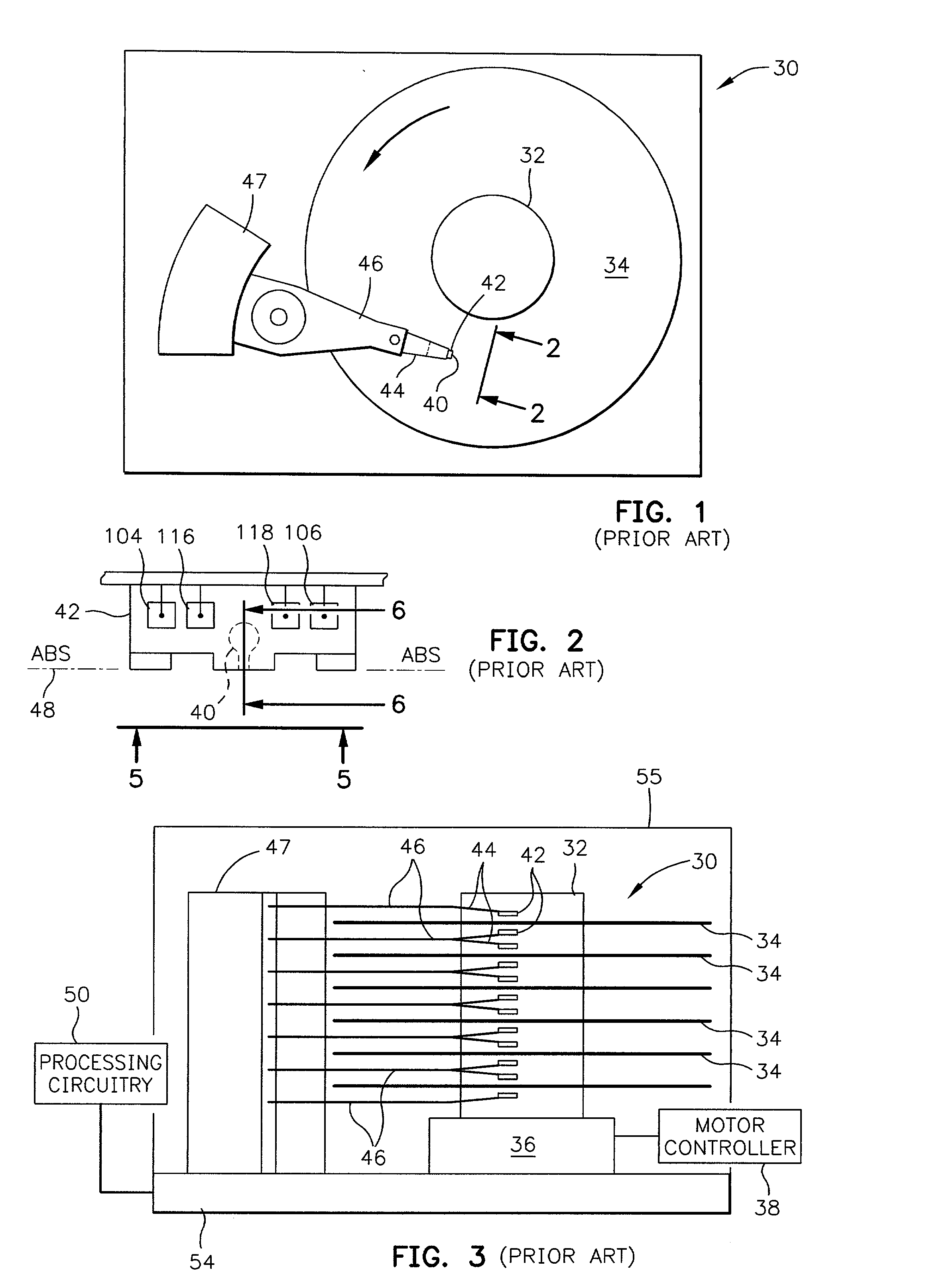
were tested at the coupon level and Examples 1 and 2 were further tested at the row level. At the coupon level a single sensor is fabricated on a glass substrate and is not lapped to the ABS. Since lapping causes the aforementioned ABS compressive stress the ABS compressive stress due to lapping is not present at the coupon level. The row level is a row of read heads including their read sensors and is taken from a slider substrate where rows and columns of such read heads have been fabricated. After dicing the row of read heads from the slider substrate, the row is lapped to the ABS which causes the aforementioned compressive stress.

[0049] At the coupon level the magnetoresistive coefficient dr / R, the intrinsic uniaxial anisotropy field H.sub.Ki, the magnetostriction .lambda. (AP) of the AP pinned layers, the magnetostriction uniaxial anisotropy field H.sub.K.lambda., the resistance of the sensor R.sub.S and the magnetostriction of the free layer .lambda. (FL) were determined and / o...


PUM

PropertyMeasurementUnit
thicknessaaaaaaaaaa
blocking temperatureaaaaaaaaaa
thicknessaaaaaaaaaa

Abstract

A spin valve sensor includes an antiparallel (AP) pinned layer structure which is self-pinned without the assistance of an antiferromagnetic (AFM) pinning layer. A free layer of the spin valve sensor has first and second wing portions which extend laterally beyond a track width of the spin valve sensor and are exchange coupled to first and second AFM pinning layers. Magnetic moments of the wing portions of the free layer are pinned parallel to the ABS and parallel to major planes of the layers of the sensor for magnetically stabilizing the central portion of the free layer which is located within the track width.

Description

[0001] The present application is related to commonly assigned co-pending U.S. patent application Ser. No. ______ by Freitag and Pinarbasi filed on ______ and entitled "HIGH MAGNETORESISTANCE SPIN VALVE SENSOR WITH SELF-PINNED ANTIPARALLEL (AP) PINNED LAYER STRUCTURE" which is incorporated in its entirety by reference herein.[0002] 1. Field of the Invention[0003] The present invention relates to a spin valve sensor with an exchange biased free layer and an antiparallel (AP) pinned layer pinned without a pinning layer and, more particularly, to the AP pinned layer structure having first and second AP pinned layers with uniaxial anisotropies that self-pin the AP pinned layer structure thereby obviating the necessity of the pinning layer.[0004] 2. Description of the Related Art[0005] The heart of a computer is a magnetic disk drive which includes a rotating magnetic disk, a slider that has write and read heads, a suspension arm above the rotating disk and an actuator arm. The suspensio...

Claims


Application Information

Patent Timeline
Patent Type & Authority Applications(United States)
IPC IPC(8): G11B5/00G11B5/012G11B5/31G11B5/39
CPCB82Y10/00G11B5/012G11B5/3163G11B2005/0016G11B5/3932G11B5/3967G11B2005/0008G11B5/3903
Inventor PINARBASI, MUSTAFA
Owner IBM CORP
Why Eureka
Try Eureka