

Surface protective film for transparent conductive substrate, and transparent conductive substrate with surface protective film
a technology of surface protective film and transparent conductive substrate, which is applied to the conductive layer on the insulating support, instruments, and textile articles on the ornamental floor, etc. it can solve the problems of inability to use the above-mentioned heating process, reduce workability, and difficulty in so as to prevent the separation of oligomers, facilitate visual inspection of the transparent conductive substrate, and ensure the effect of transparency
Inactive Publication Date: 2004-02-12
NITTO DENKO CORP
View PDF15 Cites 30 Cited by
- Summary
- Abstract
- Description
- Claims
- Application Information
AI Technical Summary
Benefits of technology
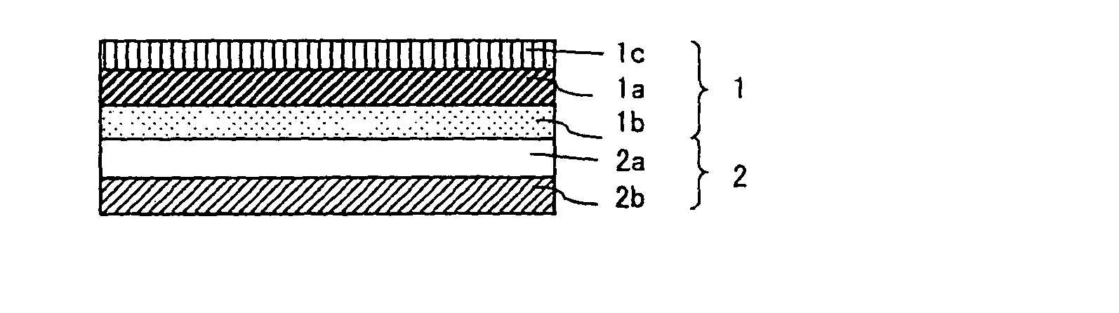
[0017] A surface prote tive film for transparent onductive substrates of the present invention (abbreviated as "surface protective film" for short hereinafter) has antistatic effect by forming an antistatic layer thereto, and further it has an especially remarkable effect that deposit of oligomers existing in a base material film to a surface of the base material film is controlled even under heated environment. Accordingly, the surface protective film does not demonstrate white turbiness and maintains sufficient transparency even after heating processes, which therefore makes visual inspection of the transparent conductive substrate easier, and prevents separation of the oligomers in the inspection process and manufacturing process of the transparent conductive substrate. Besides, the transparent conductive substrate can be protected from scratch or soil during the heating processes. Although time and effort for attaching and exchanging surface protective films before and after the heating process was needed in conventional processes, the surface protective film may be subjected to the following heating process in a state being attached on the transparent conductive substrate. Thereby, time and effort for attaching and exchanging the surface protective film may be saved, leading to remarkable improvement in workability.
Problems solved by technology
In such drying by heating processes, however, since the above-mentioned surface protective film is melted or greatly deformed, it cannot be used in the above-mentioned heating processes.
1) difficulty in visual inspection of the transparent conductive substrate;
2) considerabl decrease in workability aused by oligomers separated during the inspection of the transparent conductive substrate; and
3) possibility of ontamination given to the transparent condu tive substrate by oligomers separated even during the processes.
Since conventional surface protective films had the above-mentioned problems, the surface protective films could be used before and after heating process, but the surface protective film was difficult to be used in heating process.
Accordingly, during the heating process, transparent conductive substrates could not be protected from neither scratch nor soil, and further necessity for the surface protective film to be attached and changed in the heating process provided great complicated work, which led to decrease in working efficiency and yield, and also high manufacture cost.
Accordingly, the surface protective film does not demonstrate white turbiness and maintains sufficient transparency even after heating processes, which therefore makes visual inspection of the transparent conductive substrate easier, and prevents separation of the oligomers in the inspection process and manufacturing process of the transparent conductive substrate.
Excessively small thickness gives tendency for strength to be inadequate at a time of separation of a surfa e prot tive film 1 and for surfa protection fun tion to be inferior.
And on the ther hand, excessively large thi kness gives a t nden y to be disadvantageous in respe t of handling property or cost.
An excessively small thickness of the adhesive layer 1b makes formation of an applied layer difficult, and there is tendency for inadequate adhesive power to be demonstrated.
Excessively large thickness has tendency of providing excessive high adhesive power, which leads to tendency to give disadvantage in cost.
Method used
View moreImage
Smart ImageViewing Examples

Examples
example 1
[0062] The above-mentioned acrylic based adhesive composition was applied to a non-antistatic surface of a polyester film having an antistatic layer attached on one side (manufactured by Mitsubishi Chemical Polyester Film Corporation, T100G, thickness 38 .mu.m) with a coating machine so that a thickness after dried might be 20 .mu.m, and then dried to obtain a surface protective film.
Login to View More PUM
| Property | Measurement | Unit |
|---|---|---|
| temperature | aaaaa | aaaaa |
| thickness | aaaaa | aaaaa |
| thickness | aaaaa | aaaaa |
Abstract
To provide a surface protective film for transpar nt conductive substrates having sufficient transparency and heat resistance, and not demonstrating white turbiness, even when it is placed under a heated environment in a state where the surface protective film is attached on the transparent conductive substrate. A surface protective film for transparent conductive substrates protecting a surface on a side opposite to a conductive thin film or a surface on a side of the conductive thin film of the transparent conductive substrate, wherein an adhesive layer is formed on one side of a base material film, and an antistatic layer is formed on the other side.
Description
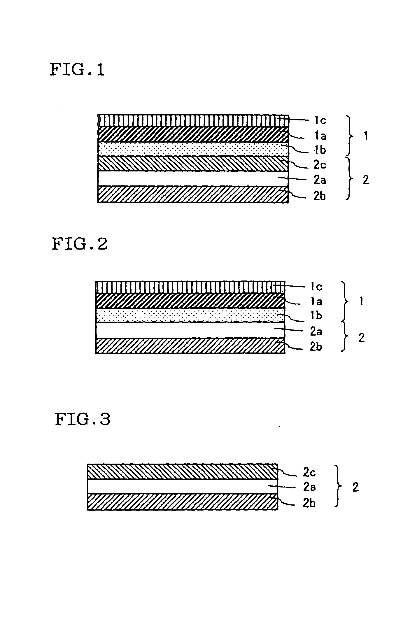
[0001] 1. Field of the Invention[0002] The present invention relates to a surface protective film used for transparent conductive substrate and to a transparent conductive substrate with the surface protective film that are widely used in a field of a transparent electrode and the like, such as liquid crystal displays, plasma display panels, touch panels, sensors, and solar cells.[0003] 2. Prior Art[0004] Generally, a transparent conductive substrate has a structure where a conductive thin film 2b comprising ITO etc. is formed on one side of a substrate 2a comprising films, such as polyesters, or glass, and hard coat layer 2c (or an anti-glare layer) on the other side is formed, as shown in FIG. 3. In such a transparent conductive substrate 2, surface protective films are conventionally used for the hard coat layer 2c on a side opposite to the conductive thin film 2b, or on the anti-glare layer in order to prev nt adhesion of foreign matter and soil. As the abov-mentioned surfa e pr...
Claims
Login to View More Application Information
Patent Timeline
 Patent Type & AuthorityApplications(United States)
IPC IPC(8): B32B7/02B32B27/00C08J7/043C08J7/044C08J7/046G02F1/1333H01B5/14
CPCB32B27/00C08J7/047Y10T428/14C08J2433/00Y10T428/28C08J2367/02Y10T428/31855Y10T428/31681C08J7/0427C08J7/043C08J7/046C08J7/044G02F1/1333B32B27/06B32B27/08B32B27/36
InventorYAMAMOTO, MITSUSHITAKADA, SHINICHIOKUMURA, KAZUHITOHAYASHI, MASAKI
OwnerNITTO DENKO CORP