Packaging of multiple active optical devices

a technology of optical devices and packaging, applied in the field of photonic devices, can solve the problems of affecting the alignment of previously bonded components, the dominance of packaging on the cost of the optoelectronic module,

Inactive Publication Date: 2004-02-12
INTEL CORP
View PDF4 Cites 97 Cited by
  • Summary
  • Abstract
  • Description
  • Claims
  • Application Information

AI Technical Summary

Problems solved by technology

Typically active alignment is a time-consuming, largely manual process that requires expensive equipment, resulting in the packaging dominating the cost of the optoelectronic module.
However heating of the substrate during bonding of subsequent components (e.g., laser dies) can affect the alignment of the previously bonded components.

Method used


Image

  • Packaging of multiple active optical devices
  • Packaging of multiple active optical devices
  • Packaging of multiple active optical devices

Examples


Embodiment Construction

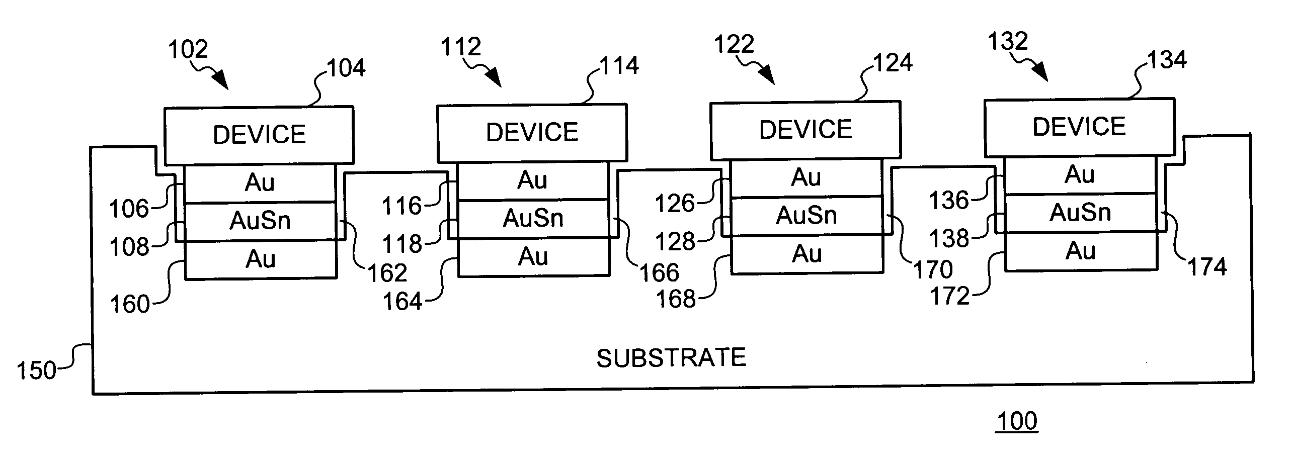
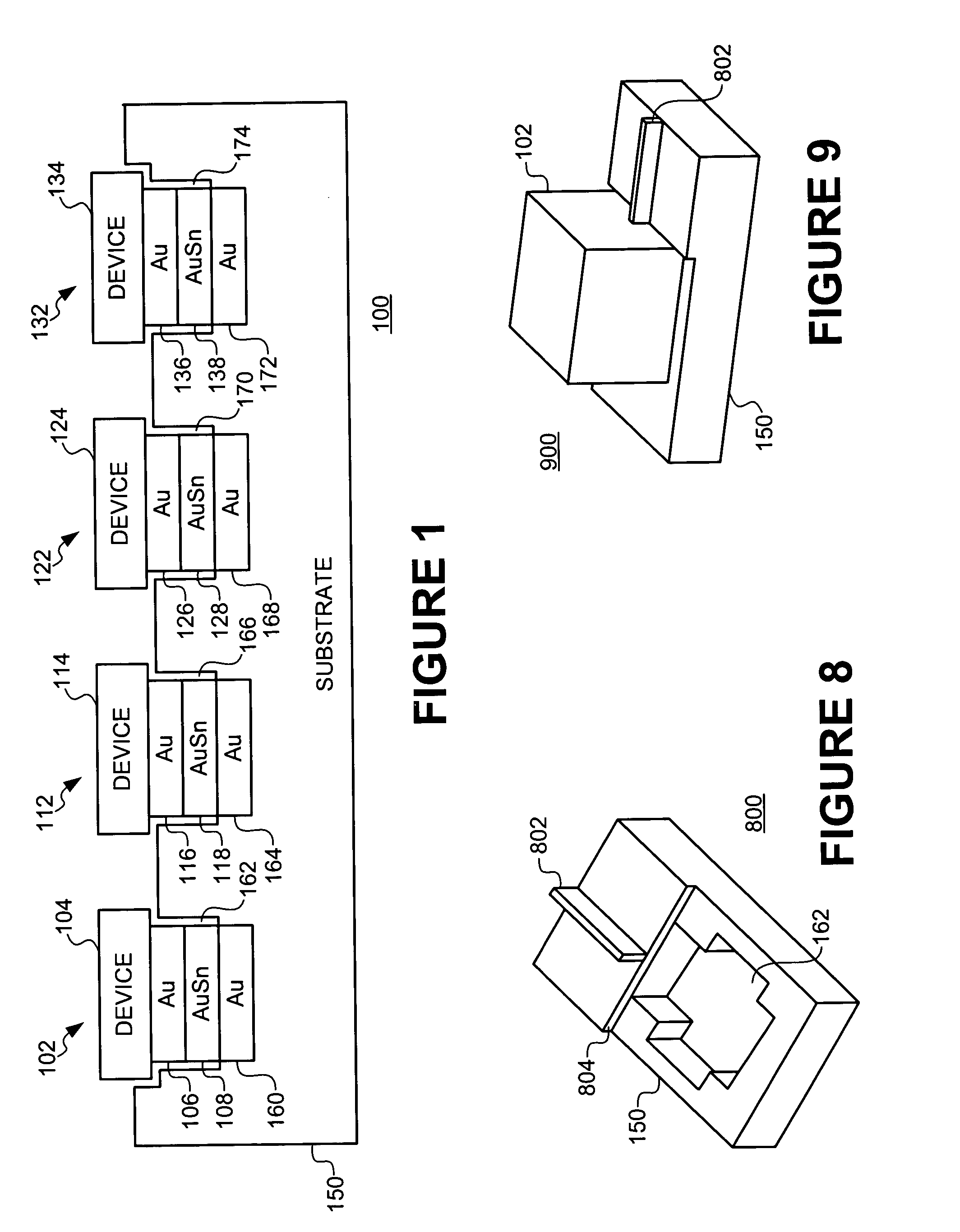
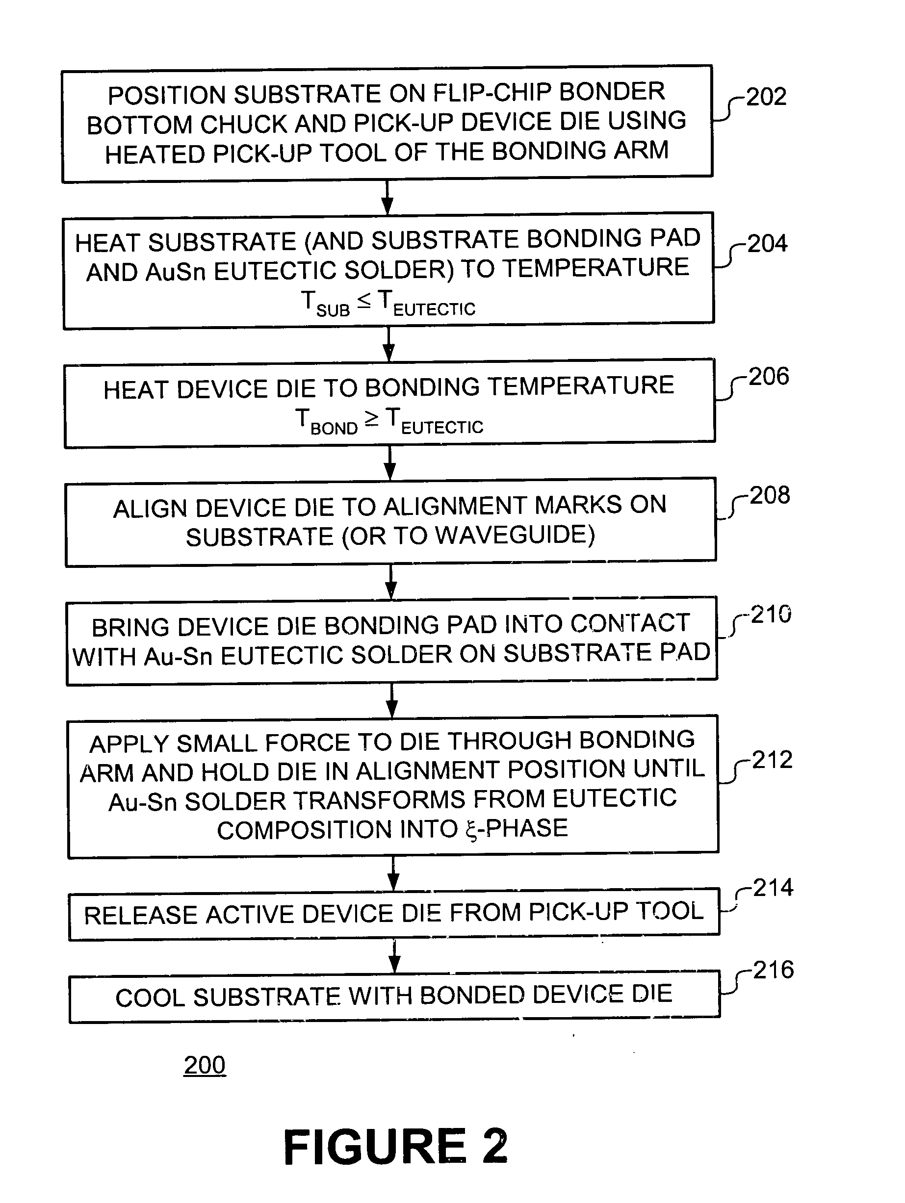
[0022] Embodiments of the present invention utilize unique properties of a gold-tin (Au--Sn) alloy system to electrically and mechanically bond active optoelectronic device dies to a substrate at different times without disturbing previously bonded dies. In the following description, numerous specific details, such as particular processes, materials, devices, and so forth, are presented to provide a thorough understanding of embodiments of the invention. One skilled in the relevant art will recognize, however, that the invention can be practiced without one or more of the specific details, or with other methods, components, etc. In other instances, well-known structures or operations are not shown or described in detail to avoid obscuring various embodiments of the present invention.

[0023] Some parts of the description will be presented using terms such as waveguide, silicon, solder, active optoelectronic device, multiplexer, eutectic, and so forth. These terms are commonly employed...


PUM


Abstract

A cost effective method is provided for assembly of hybrid optoelectronic circuits requiring flip-chip bonding of multiple active optoelectronic devices onto common substrate or optical bench platform with fine pitch and high accuracy "after-bonding" alignment to the alignment features on substrate and / or to other elements of the hybrid circuit. A Flip-Chip Bonder equipped with high precision Bonding Arm and optical and mechanical system, heated substrate chuck and heated pick-up tool may be used both for alignment and thermal bonding of active component dies to corresponding bonding pads on the common substrate using gold-tin (Au-Sn) solder disposed between die bonding pad and the corresponding substrate bonding pad. During bonding of the first die, tin (Sn) diffuses from a eutectic composition of gold-tin (Au-Sn) solder to (gold (Au) on) the die-bonding pad and / or (gold (Au) on) the substrate bonding-pad resulting in transformation of the Au-Sn eutectic composition to a zeta-phase composition having much higher melting temperature as compared to that of a eutectic composition. As bonding of one or more subsequent dies is performed at temperatures equal to or slightly higher than the melting temperature of a eutectic composition and significantly lower than the melting temperature of a zeta-phase composition, the gold-tin (Au-Sn) solder at the bond of previously attached die does not melt and, consequently, the alignment is not compromised.

Description

[0001] The present application is related to U.S. patent application Ser. No. 10 / 109,166 [Attorney Docket No. 42390.P13372], filed Mar. 27, 2002 entitled "Packaging of Multiple Active Optical Devices," with inventors Mikhail Naydenkov, Sivasubramaniam Yegnanarayanan and Quyen Huynh.[0002] 1. Field of the Invention[0003] The present invention is related to photonic devices and, in particular to hybrid integrated optoelectronic circuits and optical packaging[0004] 2. Background Information[0005] Hybrid integrated optoelectronic circuits are commonly fabricated using discrete active and passive photonic devices and electronic devices. Active photonic devices commonly include edge-emitting lasers such as Fabry-Perot (FP) & distributed feedback lasers (DFB), vertical cavity surface-emitting lasers (VCSEL), electro-absorption modulated lasers (EML), photodetectors, semiconductor optical amplifiers, electro-absorption modulators, and other discrete photonic devices. Active optoelectronic (...

Claims


Application Information

Patent Timeline
Patent Type & Authority Applications(United States)
IPC IPC(8): G02B6/12G02B6/28G02B6/34H05K3/34
CPCG02B6/2813G02B6/4238G02B6/12007H05K3/3463G02B6/12004H05K3/3436
Inventor NAYDENKOV, MIKHAILYEGNANARAYANAN, SIVASUBRAMANIAMHUYNH, QUYEN
Owner INTEL CORP
Why Eureka
Try Eureka