Apparatuses and methods for treating a silicon film

Inactive Publication Date: 2004-04-01
WALDHAUER ANN +1
View PDF0 Cites 51 Cited by
  • Summary
  • Abstract
  • Description
  • Claims
  • Application Information

AI Technical Summary

Problems solved by technology

Most of the methods of fabricating SOI substrates have some common disadvantages, non-uniform thickness and non-smooth surface.
Plasma polishing introduces non-uniformity and some surface damages associated with substrate with chemical mechanical polishing.
GCIB process gives good thickness control but a film processed under a GCIB process does not

Method used


Image

  • Apparatuses and methods for treating a silicon film
  • Apparatuses and methods for treating a silicon film
  • Apparatuses and methods for treating a silicon film

Examples


Embodiment Construction

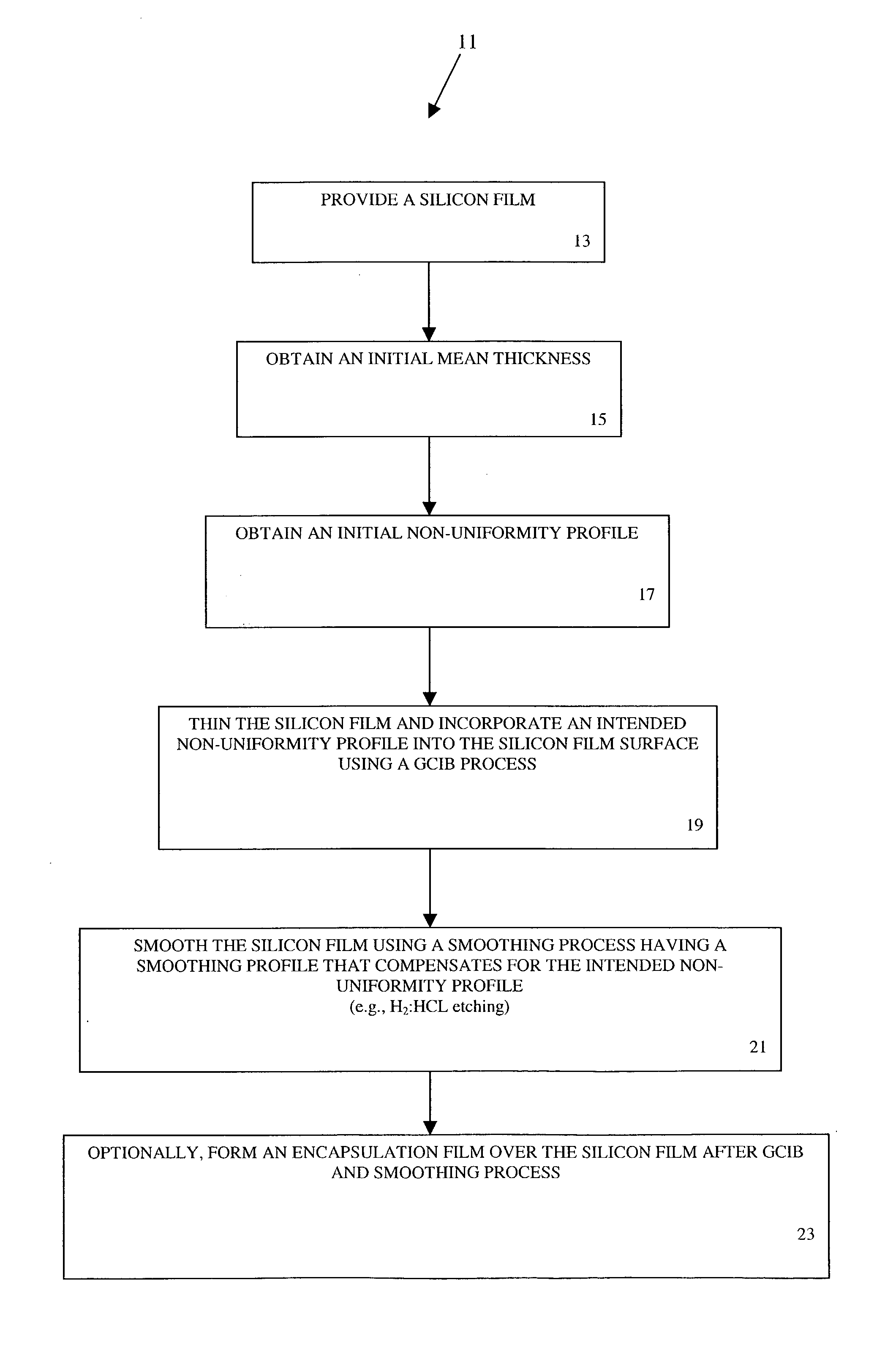
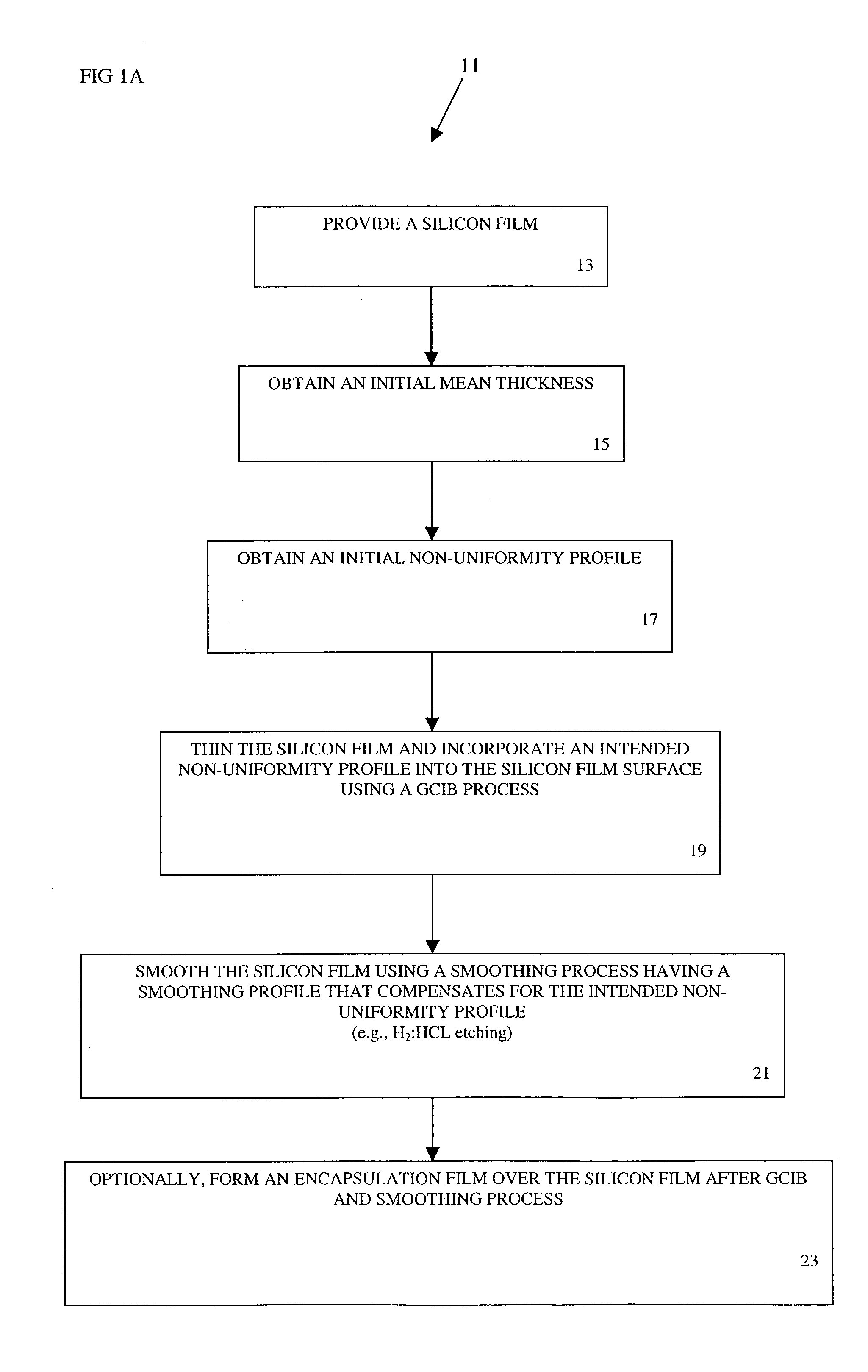
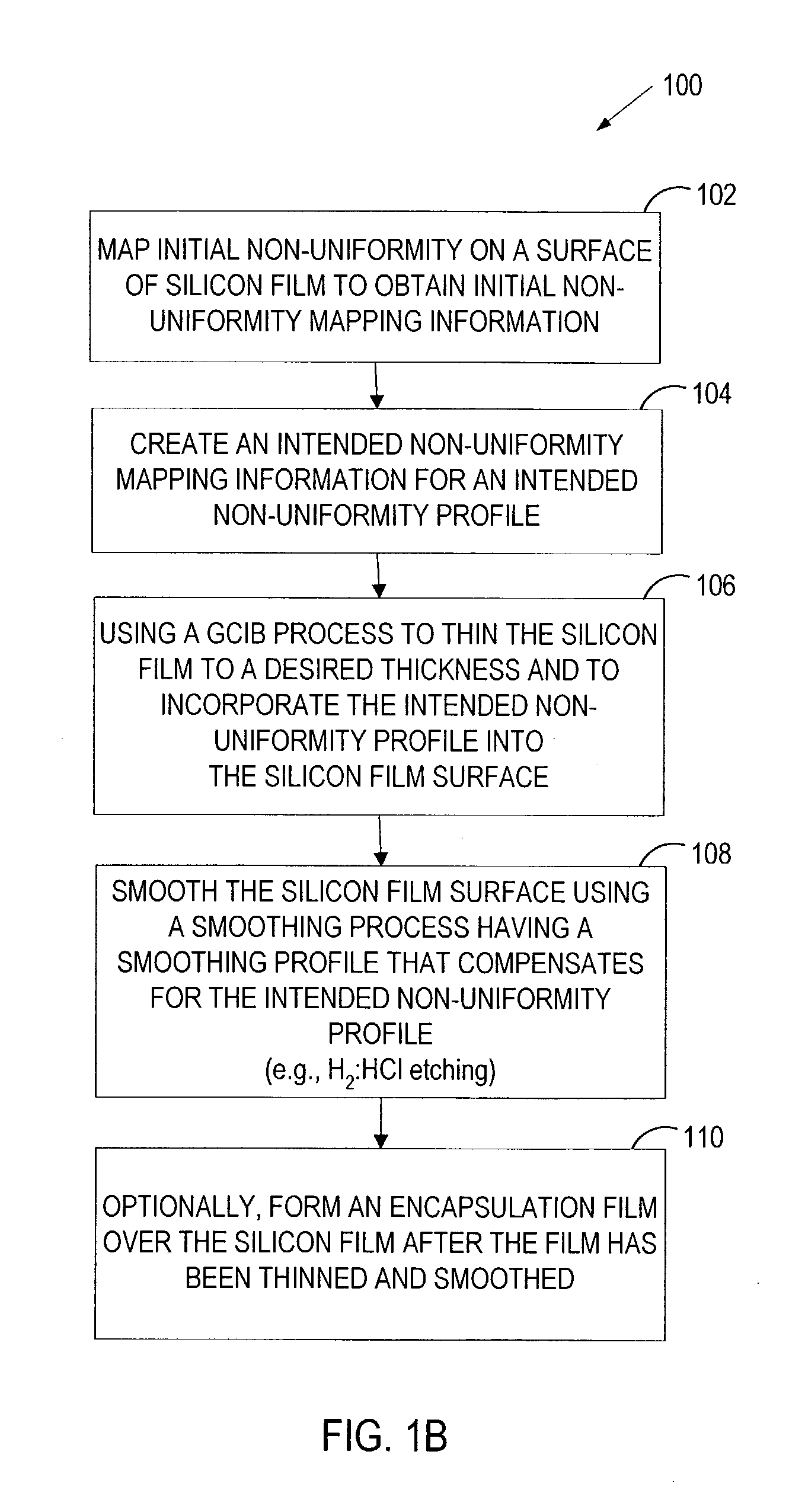
[0025] The present invention describes methods and apparatuses for treating a silicon film, which is useful for fabricating a silicon-on-insulator (SOI) substrate. In the following description numerous specific details are set forth in order to provide a through understanding of the present invention. One skilled in the art will appreciate that these specific details are not necessary in order to practice the present invention. In other instances, well known equipment features and processes have not been set forth in detail in order to not unnecessarily obscure the present invention.

[0026] The exemplary embodiments of the present invention include methods and apparatuses for treating a silicon film. Treating the silicon film includes first thinning the silicon film to a thickness and then smoothing the silicon film surface. Optionally, the silicon film is protected with an encapsulation layer after being thinned and smoothed. A silicon film that can be treated using the exemplary em...


PUM

PropertyMeasurementUnit
Timeaaaaaaaaaa
Timeaaaaaaaaaa
Angleaaaaaaaaaa

Abstract

A method of treating a silicon film on a substrate. A silicon film is provided. The silicon film is thinned using a gas cluster ion beam (GCIB) process. The silicon film surface then is smoothed out using an etching process or an annealing process. Optionally, an encapsulation film is formed on the silicon film after the GCIB process and the etching process or the annealing process.

Description

[0001] 1. Field of the Invention[0002] The present invention relates to treating a silicon film and more specifically to methods and apparatuses for thinning and smoothing a silicon film.[0003] 2. Discussion of Related Art[0004] During the past several years, demand for silicon on insulator (SOI) substrates has greatly increased. Devices such as transistors and capacitors typically formed on a silicon wafer can be formed on the SOT substrates. SOI substrates are in high demand because they have low current leakage, which allows electronic devices created on the SOI substrates to consume less power. Additionally, the electronic devices created on the SOI substrates can be made smaller.[0005] An SOI substrate can be created using several processes. For example, an SOI substrate may be fabricated using a separation by implant oxygen (SIMOX) process, of bond and etch back (BE) process, a hydrogen implant and release silicon process (sometimes known as SmartCut.RTM.) ("SmartCut.RTM." is ...

Claims


Application Information

Patent Timeline
IPC IPC(8): H01L21/302H01L21/306H01L21/3065H01L21/762
CPCH01J2237/0812H01L21/76254H01L21/3065H01L21/30604
Inventor WALDHAUER, ANNCOMITA, PAUL B.
Owner WALDHAUER ANN
Why Eureka
Try Eureka