

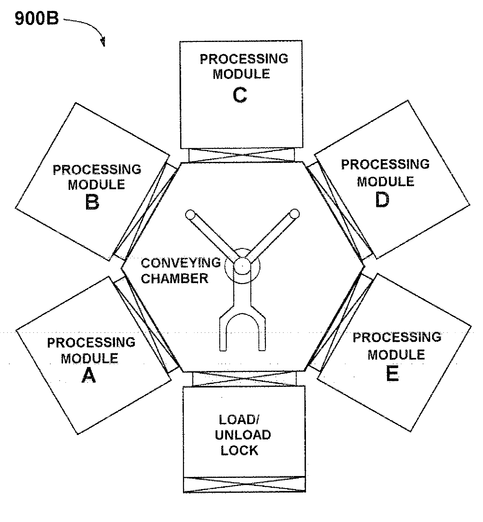
GCIB Cluster Tool Apparatus and Method of Operation
a technology of clustering tool and tool body, which is applied in the direction of vacuum evaporation coating, chemical vapor deposition coating, coating, etc., can solve the problems of interconnect wire failure, copper wire surface, and need to carry ever-higher electrical current in smaller and smaller sizes, so as to reduce the pressure atmosphere
- Summary
- Abstract
- Description
- Claims
- Application Information
AI Technical Summary
Benefits of technology
Problems solved by technology
Method used
Image

Examples
first embodiment
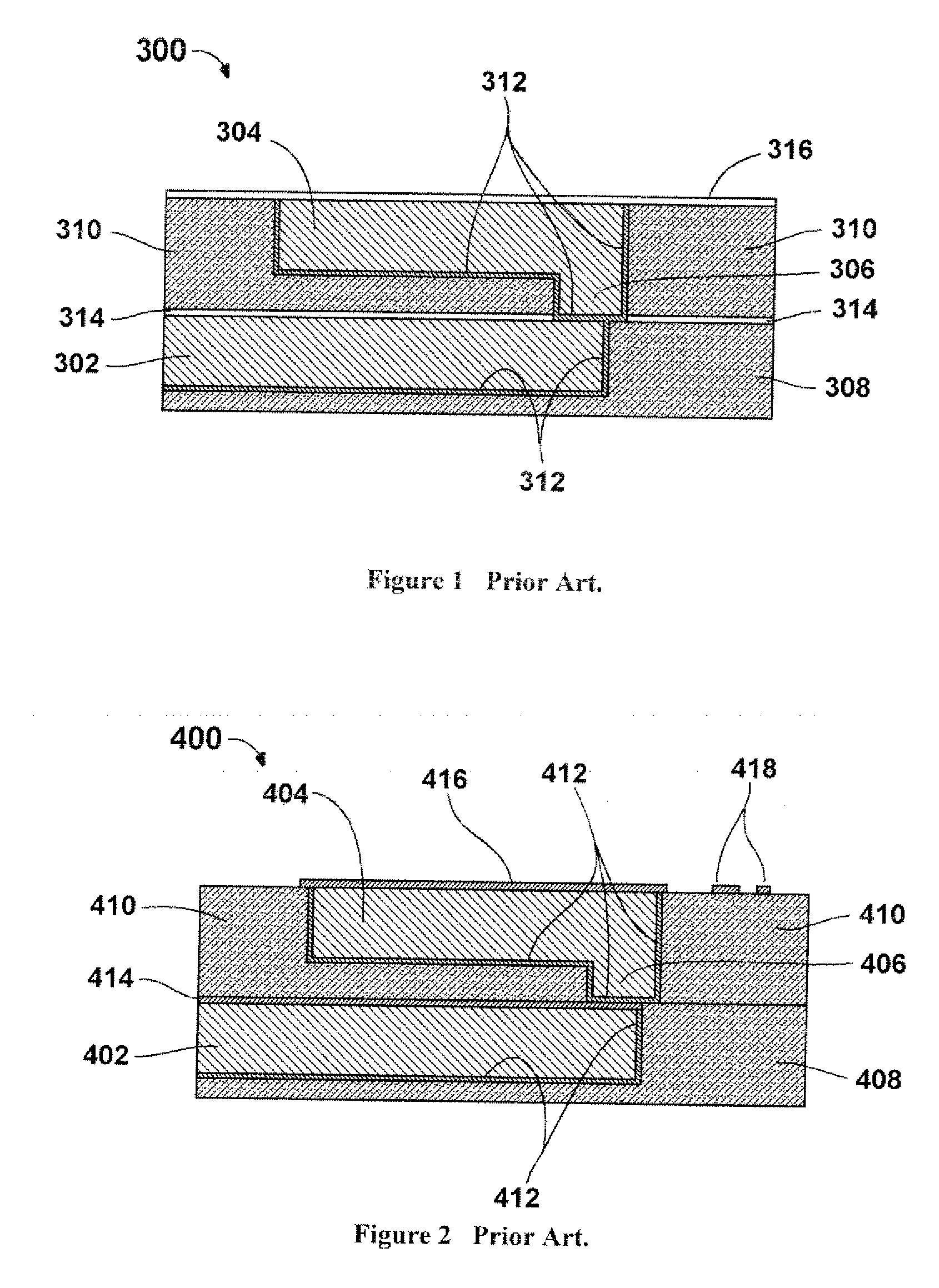
[0047]FIG. 4A is a schematic showing a wiring scheme 500 of a copper interconnect capped using GCIB infusion according to the invention (showing for example, not for limitation, two copper wire layer interconnect levels). The schematic shows a substrate 501 supporting a first copper wire layer 502, a second copper wire layer 504, and copper via structure 506 connecting the two copper layers, each of which may be formed using conventional techniques. The substrate 501 is typically a semiconductor substrate containing active and / or passive elements (possibly including lower interconnect levels) requiring electrical interconnection. The sidewalls and bottoms of both copper wire layers 502 and 504 and the via structure 506 are lined with a TaN / Ta or other conventional barrier layer 512, which may be formed using conventional techniques. First inter-level dielectric layer 508 and second inter-level dielectric layer 510 provide electrical insulation between the copper wire layers and othe...
third embodiment
[0065]FIG. 6A is a schematic showing a wiring scheme 700 of a copper interconnect capped using GCIB infusion according to the invention (showing for example, not for limitation, two copper wire layer interconnect levels). The schematic shows a substrate 701 supporting a first copper wire layer 702, a second copper wire layer 704, and copper via structure 706 connecting the two copper layers, each of which may be formed using conventional techniques. The substrate 701 is typically a semiconductor substrate containing active and / or passive elements (possibly including lower interconnect levels) requiring electrical interconnection. The sidewalls and bottoms of both copper wire layers 702 and 704 and the via structure 706 are lined with a barrier layer 712, which may be formed using conventional techniques, First inter-level dielectric layer 708 and second inter-level dielectric laver 710 provide electrical insulation between copper wires and may be formed using conventional techniques...
fourth embodiment
[0073]FIG. 7A is a schematic showing a wiring scheme 800 of a copper interconnect capped using GCIB infusion according to the invention (showing for example, not for limitation, two copper wire layer interconnect levels). The schematic shows a substrate 801 supporting a first copper wire layer 802, a second copper wire layer 804, and copper via structure 806 connecting the two copper layers, each of which may be formed using conventional techniques. The substrate 801 is typically a semiconductor substrate containing active and / or passive elements (possibly including lower interconnect levels) requiring electrical interconnection. The sidewalls and bottoms of both copper wire layers 802 and 804 and the via structure 806 are lined with a barrier layer 812, which may be formed using conventional techniques. First inter-level dielectric laver 808 and second inter level dielectric layer 810 provide electrical insulation between copper wires and may be formed using conventional techniques...
PUM
| Property | Measurement | Unit |
|---|---|---|
| Dielectric polarization enthalpy | aaaaa | aaaaa |
| Pressure | aaaaa | aaaaa |
Abstract
Description
Claims
Application Information