GCIB liner and hardmask removal process

a technology of hardmask removal and gcib liner, which is applied in the direction of semiconductor/solid-state device manufacturing, basic electric elements, electric devices, etc., can solve the problems of limited cmp, worse uniformity, and non-uniform surface uniformity not within acceptable tolerances

Active Publication Date: 2007-05-24
TWITTER INC
View PDF24 Cites 30 Cited by
  • Summary
  • Abstract
  • Description
  • Claims
  • Application Information

AI Technical Summary

Benefits of technology

[0011] In a third aspect of the invention a system, a device, comprises a smoothed surface with variations and roughness of less than 1 nm (nanometer) in height across the chip.

Problems solved by technology

CMP, though, is limited because the physical polish often generates scratches, erosion, or other surface defects on the wafer surface.
Additionally, the polish rate depends upon the pattern density factor; thus the longer the polish, the worse the uniformity.
This non-uniformity of the surface is not within the acceptable tolerances for processing the very thin wire levels of emerging fabrication methods.

Method used


Image

  • GCIB liner and hardmask removal process
  • GCIB liner and hardmask removal process
  • GCIB liner and hardmask removal process

Examples


Embodiment Construction

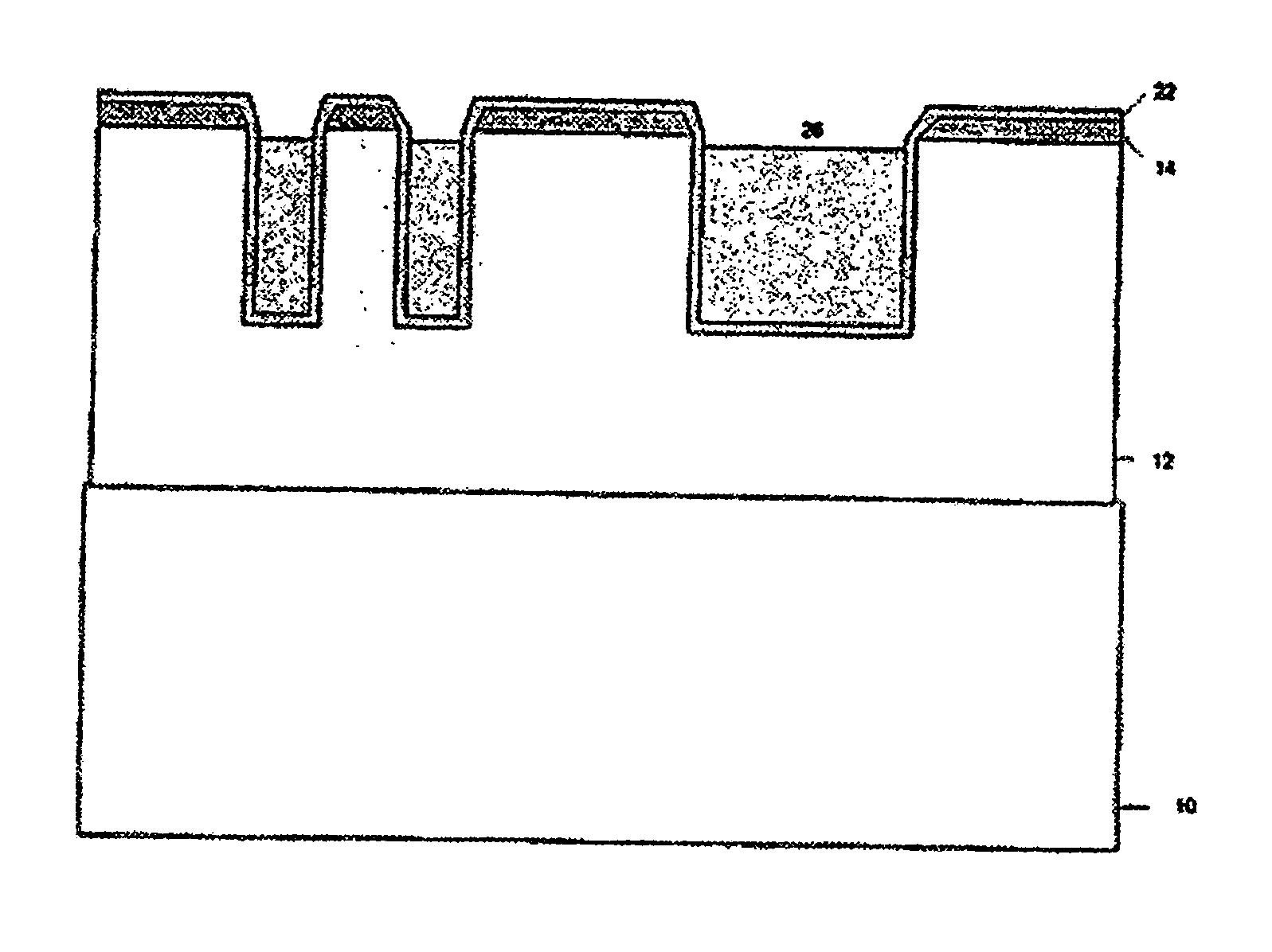
[0017] The invention is generally directed to a system and method of etching and smoothing of surfaces during semiconductor fabrication by the process of gas cluster ion beam (GCIB) etching. GCIB etching by the method of the present invention achieves a uniform planar smoothed surface (compared to conventional processes), having extremely uniform line resistance across the wafer. In comparison with existing methods of smoothing of surfaces, the inventive process is more easily controlled than, for example, reactive ion etching (RIE).

[0018] Additionally, the inventive process produces a more uniform and scratch-free surface, without dependency on pattern density, than conventional chemical mechanical polishing (CMP). In particular, the method of the present invention is well suited to application on surfaces that include complex structures such as very large scale integration and ultra large scale integration. The method of the present invention may produce a smoothed surface with v...


PUM

PropertyMeasurementUnit
dielectric constantaaaaaaaaaa
heightaaaaaaaaaa

Abstract

A method comprises depositing a dielectric film layer, a hard mask layer, and a patterned photo resist layer on a substrate. The method further includes selectively etching the dielectric film layer to form sub-lithographic features by reactive ion etch processing and depositing a barrier metal layer and a copper layer. The method further includes etching the barrier metal layer and hard mask layer by gas cluster ion beam (GCIB) processing.

Description

DESCRIPTION [0001] 1. Field of the Invention [0002] The invention generally relates to the field of semiconductor fabrication, and more particularly, to an integrated fabrication process of etching and smoothing surfaces using gas cluster ion beam (GCIB) etching. [0003] 2. Background Description [0004] Surfaces of microelectronic materials such as semiconductors, dielectrics, and metals (often as thin films on a substrate) are generally planarized after their fabrication. The close proximity of microelectronic components, either as multiple layers or as interacting and interconnected subcomponents, requires a high degree of uniformity of the surface. Advances in semiconductor technology have seen the advent of very large scale integration (VLSI) and ultra large scale integration (ULSI) circuits, resulting in the integration of very many more devices in smaller areas on a semiconductor substrate. [0005] The greater device densities require greater degrees of planarity to permit the h...

Claims


Application Information

Patent Timeline
Patent Type & Authority Applications(United States)
IPC IPC(8): H01L21/76
CPCH01L21/31116H01L21/32136H01L21/76802H01L21/7684
Inventor CHEN, SHYNG-TSONG T.FITZSIMMONS, JOHN A.PONOTH, SHOM S.SPOONER, TERRY A.
Owner TWITTER INC
Why Eureka
Try Eureka