Thin film transistor, production method and production apparatus therefor

a technology of thin film transistor and production method, which is applied in the direction of transistors, electrical equipment, semiconductor devices, etc., can solve the problems of increasing leakage current, not keeping the interface between the gate insulating film and the semiconductor layer clean, and not giving the desired characteristics of the thin film transistor

Inactive Publication Date: 2006-06-15
CANON KK
View PDF7 Cites 41 Cited by
  • Summary
  • Abstract
  • Description
  • Claims
  • Application Information

AI Technical Summary

Problems solved by technology

H06-045605 can produce the thin film transistor with the high mobility of a carrier, which originates in the flatness of a silicon nitride film that is a gate insulating film, but has a problem that the obtained thin film transistor may show low reliability because the silicon nitride film contains a low volume ratio of N to Si and consequently has low resistivity and withstand voltage.
H05-013763 uses a spin coating technique for coating, for instance, a silanol-based compound on the surface of an insulating film, in the step of flattening the gate insulating film, consequently can not keep an interface be

Method used


Image

  • Thin film transistor, production method and production apparatus therefor
  • Thin film transistor, production method and production apparatus therefor
  • Thin film transistor, production method and production apparatus therefor

Examples


embodiment 1

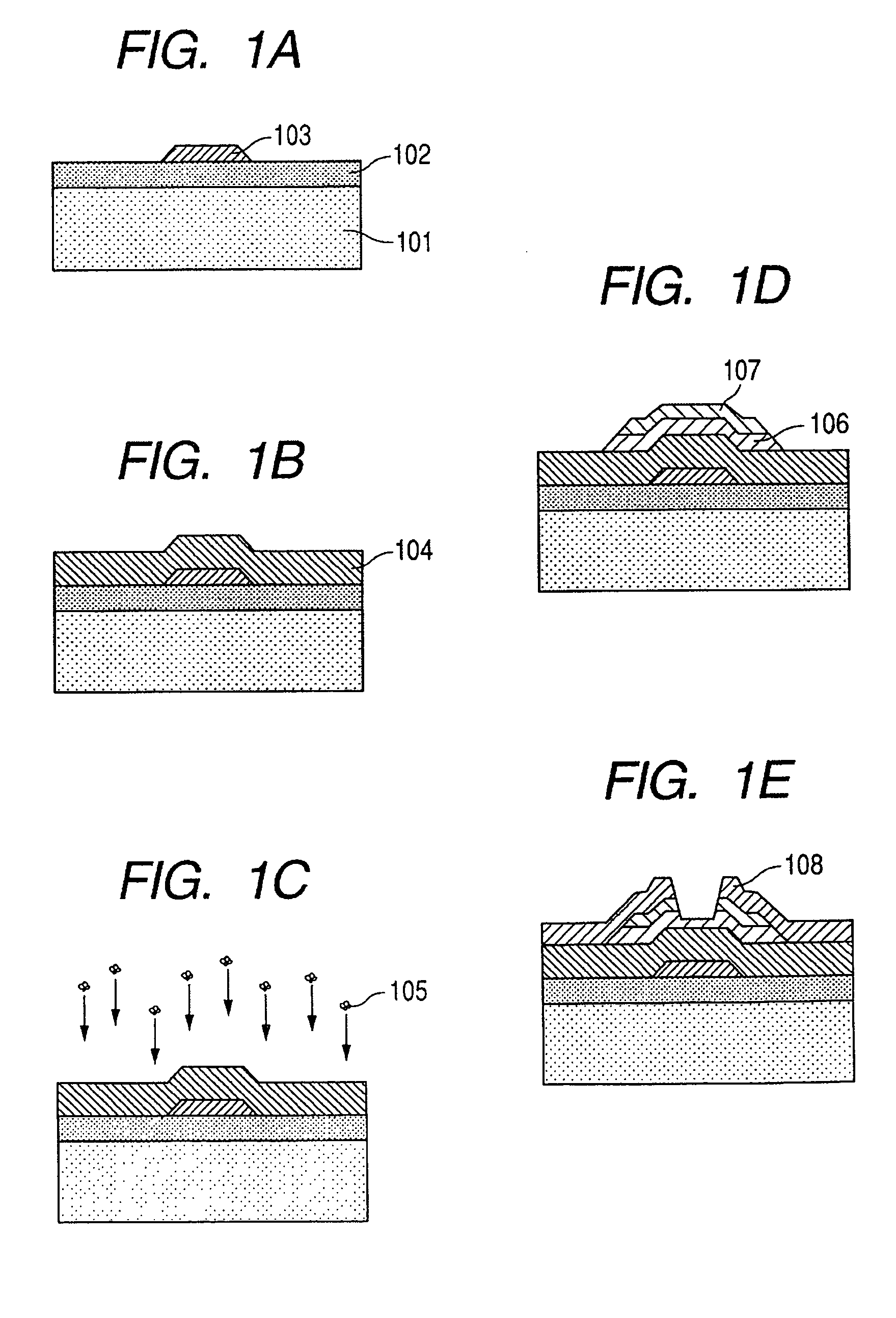
[0028]FIGS. 1A, 1B, 1C, 1D and 1E show sectional views for describing a production method according to the present embodiment. In FIG. 1A, a barrier layer 102 and a gate electrode 103 are formed on an insulation substrate 101. The barrier layer is provided as needed, in order to prevent impurities in the substrate from diffusing to an element side. The films are produced by using the normal steps of: forming the barrier layer 102; forming an electroconductive film on the barrier film, which will become a gate electrode 103; and forming the gate electrode 103 by using a normal photolithographic technology. A silicon oxide film or a silicon nitride film is used for the barrier layer, and may have a thickness of about 50 to 200 nm. The usable gate electrode has the film thickness preferably of 50 to 500 nm and more preferably of 70 to 200 nm, and is formed of at least one layer made of an electroconductive material such as Al, Cr, W, Mo, Ti, Ta, AlTi and AlNd.

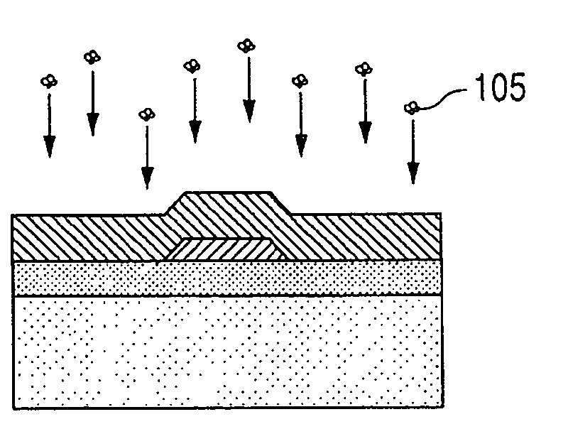
[0029] Subsequently, as s...

embodiment 2

[0052] In the present embodiment, the same description as in Embodiment 1 will be omitted.

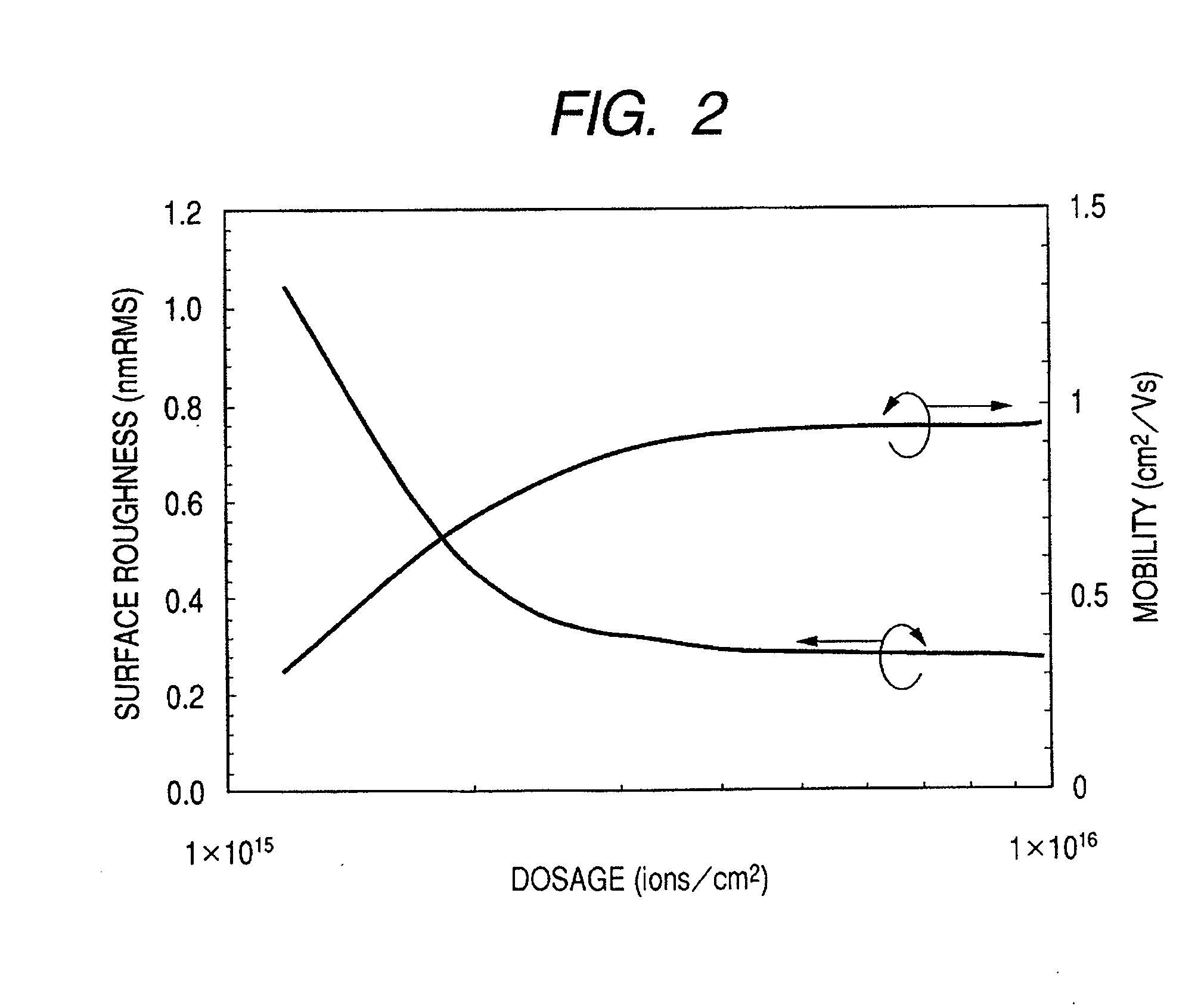
[0053] In the present embodiment as well, a thin film transistor is formed by the steps as described in FIGS. 1A, 1B, 1C, 1D and 1E. In the present embodiment, nitrogen is used for a gas cluster ion as a gaseous species. A substrate having a gate insulating film formed thereon was irradiated with nitrogen cluster ions accelerated into the energy of 5 keV at the dosage of 7×10¹⁵ ions / cm2 (cf. FIG. 3), in a gas cluster ion beam irradiation chamber. The gate insulating film showed the surface roughness of 0.3 nm by RMS after having been irradiated.

[0054] The thin film transistor produced with the above described method showed an improved mobility of a carrier, because of having a flat and clean interface between a gate insulating film and a semiconductor film; and showed improved reliability because the N / Si ratio of a silicon nitride film increased. The improvement in the reliability is particu...

embodiment 3

[0055] In the present embodiment, a silicon oxide film is used for a gate insulating film. A silicon oxide film was formed as a gate insulating film with a PECVD process which employed TEOS (tetra ethyl ortho silicate) and oxygen as inflow gaseous species and controlled the flow ratio of TEOS to oxygen to 1:20. The formed silicon oxide film had the thickness of 150 nm. After that, a substrate having the gate insulating film formed thereon was irradiated with oxygen cluster ions accelerated to the energy of 5 keV, at the dosage of 7×10¹⁵ ions / cm2 (cf. FIG. 4), in a gas cluster ion beam irradiation chamber. The surface roughness of a gate insulating film after having been irradiated was 0.23 nm by RMS.

[0056] The thin film transistor produced with the above described method showed an improved mobility of a carrier, because of acquiring a flat and clean interface between a gate insulating film and a semiconductor film; and showed an improved reliability, because the O / Si ratio of a sil...


PUM

PropertyMeasurementUnit
Electric potential / voltageaaaaaaaaaa
Electrical resistivityaaaaaaaaaa
Mobilityaaaaaaaaaa

Abstract

A thin film transistor produced through flattening a gate insulating film acquires the high mobility of a carrier, but has a problem of occasionally showing low resistivity, low withstanding voltage, and consequent low reliability. The present invention solves the above described problem and provides a thin film transistor having the high mobility, the high resistivity, the high withstanding voltage and the high reliability. The present invention also provides a method for producing a thin film transistor having a semiconductor film formed on a gate insulating film thereon, which has the steps of: forming the gate insulating film; and flattening a surface of the gate insulating film by irradiating the surface of the gate insulating film with a gas cluster ion beam.

Description

BACKGROUND OF THE INVENTION [0001] 1. Field of the Invention [0002] The present invention relates to a thin film transistor and a production method therefor. [0003] 2. Related Background Art [0004] Conventionally, for a semiconductor device for driving a liquid crystal display and a semiconductor device for driving a photovoltaic device, a thin film transistor (TFT: Thin Film Transistor: hereafter abbreviated as TFT) has been used. As for the structure, a coplaner type, a stagger type and a reversed stagger type are proposed. [0005] Such TFTs are required to have various functions according to applications. Particularly, a large screen and a high definition liquid crystal display used in recent years have to write information on one pixel in short time, so that a thin film transistor used therein is absolutely required to improve its writing capability, in other words, to enhance the mobility of a carrier. [0006] Japanese Patent Application Laid-Open No. H06-045605 discloses a metho...

Claims


Application Information

Patent Timeline
IPC IPC(8): H01L29/786H01L21/84H01L21/67
CPCH01L29/4908Y10T29/41H01L29/78609H01L29/66765
Inventor FUKUMIYA, YOICHISAITO, TETSUROSHOJI, TATSUMI
Owner CANON KK
Why Eureka
Try Eureka