Field effect transistor with etched-back gate dielectric

a dielectric and field effect technology, applied in the field of field effect transistors, can solve the problems of difficulty in achieving the desired nitrogen concentration profil

Active Publication Date: 2006-07-04
GLOBALFOUNDRIES US INC
View PDF2 Cites 44 Cited by
  • Summary
  • Abstract
  • Description
  • Claims
  • Application Information

AI Technical Summary

Problems solved by technology

Unintended thickness variations as small as one angstrom (A) can produce order of magnitude variations in the leakage of a 15A gate dielectric, a highly undesirable situation.
However, it can be difficult to achieve the desired concentration profile of nitrogen (quantity and depth distribution) without damaging the high-k film and / or semiconductor substrate.

Method used


Image

  • Field effect transistor with etched-back gate dielectric
  • Field effect transistor with etched-back gate dielectric
  • Field effect transistor with etched-back gate dielectric

Examples


example 1

An Approximately 5 nm HfO2 Film is Thinned to About 3 nm Without Substantial Roughening

[0039]An approximately 4.5 nm thick film of HfO2, impervious to dHF as-deposited, was given an Ar reactive ion etch (RIE) damage treatment in a LAM9400 RIE tool. The conditions were: an Ar pressure of 5 mTorr, an Ar flow of 60 sccm, a top power of 100 W, a bottom power of 300 W, and a self-bias of 160 Vdc, for 10 seconds. The RIE treatment removed about 0–0.5 nm of HfO2. A 30 sec treatment in dHF reduced the film thickness to about 3.2 nm. FIGS. 5A–5B show atomic force microscope (AFM) images of the film before (FIG. 5A) and after (FIG. 5B) the damage / wet etch process. Film roughness was similar before and after the thinning: rms / peak-to-valley roughness was about 2.2 / 7.6 A (before) and about 2.1 / 7.8 A (after).

example 2

An Approximately 3 nm HfO2 Film is Thinned to About 1 nm With Some Roughening

[0040]An approximately 3.1 nm thick film of HfO2 was annealed in N2 at 700° C. for 30 sec to make it impervious to dHF. The film was then given an Ar RIE damage treatment in a LAM9400 RIE tool. The conditions were: an Ar pressure of 5 mTorr, an Ar flow of 60 sccm, a top power of 100 W, a bottom power of 100 W, and a self-bias of 60 Vdc for 30 sec. The RIE treatment removed about 0.6 nm of HfO2. A 2 min treatment in dHF reduced the film thickness to about 1.1 nm. FIGS. 5C–5D show AFM images of the film before (FIG. 5C) and after (FIG. 5D) the damage / wet etch process. Film roughness was substantially greater after the thinning: rms / peak-to-valley roughness was about 2.2 / 6.2 A (before) and about 4.7 / 19 A (after).

[0041]This roughening was attributed to an insufficiently aggressive crystallization anneal (700° C. at 30 seconds in N2), which left the bottom 1–2 nm of the HfO2 film a mixture of crystalline regions...

example 3

A HfO2 Film is Thinned from About 3 nm to About 2 nm By Ar Sputter Etching Without Substantial Roughening

[0042]An approximately 3 nm thick film of HfO2, etchable in dHF as-deposited, was given an Ar RIE thinning treatment in a Unaxis 790 series RIE tool. The conditions were: an Ar pressure of 20 mTorr, an Ar flow of 20 sccm, a bottom power of 200 W, and a self-bias of 420 Vdc, for 2 min. The RIE treatment removed about 1.0 nm of HfO2. The film was annealed in N2 at 700° C. for 1 min to repair any residual RIE damage. FIGS. 5E–5F show AFM images of the film before (FIG. 5E) and after (FIG. 5F) the thinning process. Film roughness was similar before and after thinning: rms / peak-to-valley roughness was about 2.2 / 6.5 A (before) and about 2.1 / 6.6 A (after).


PUM


Abstract

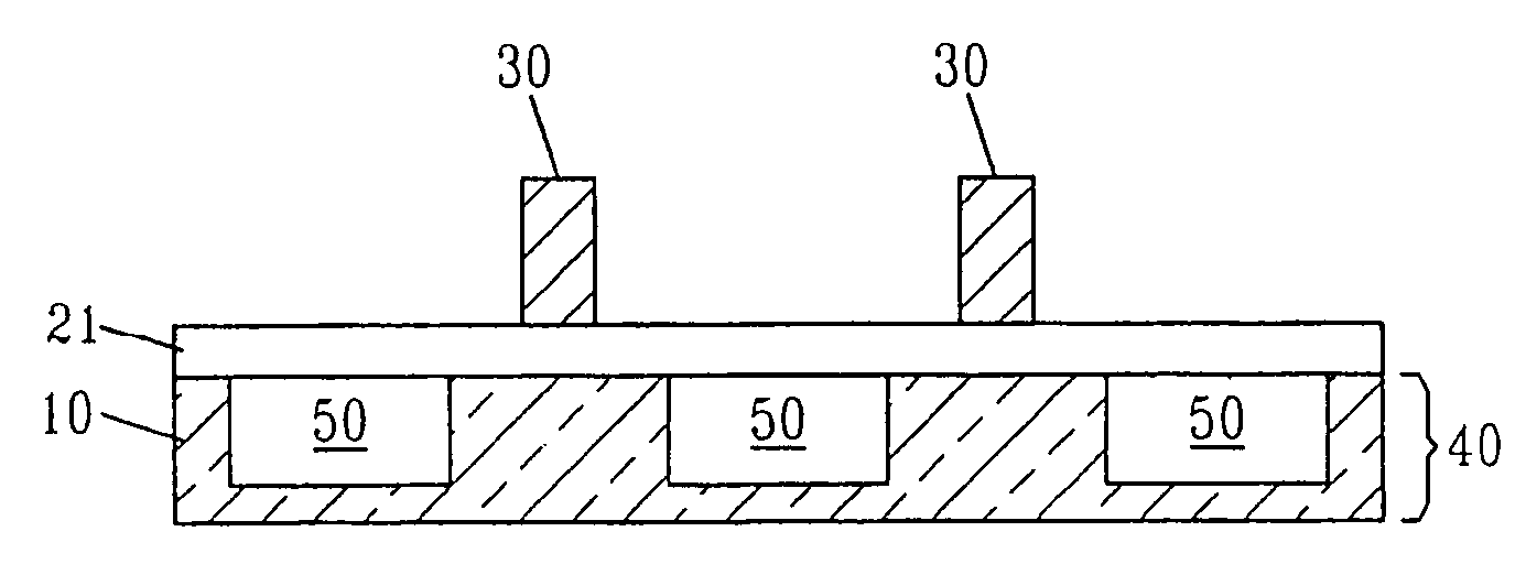
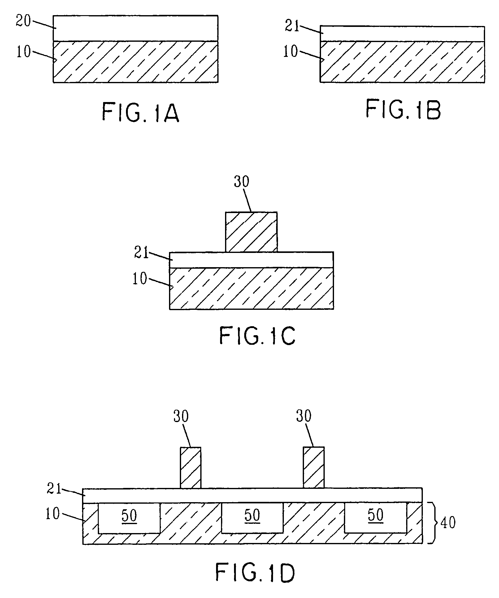
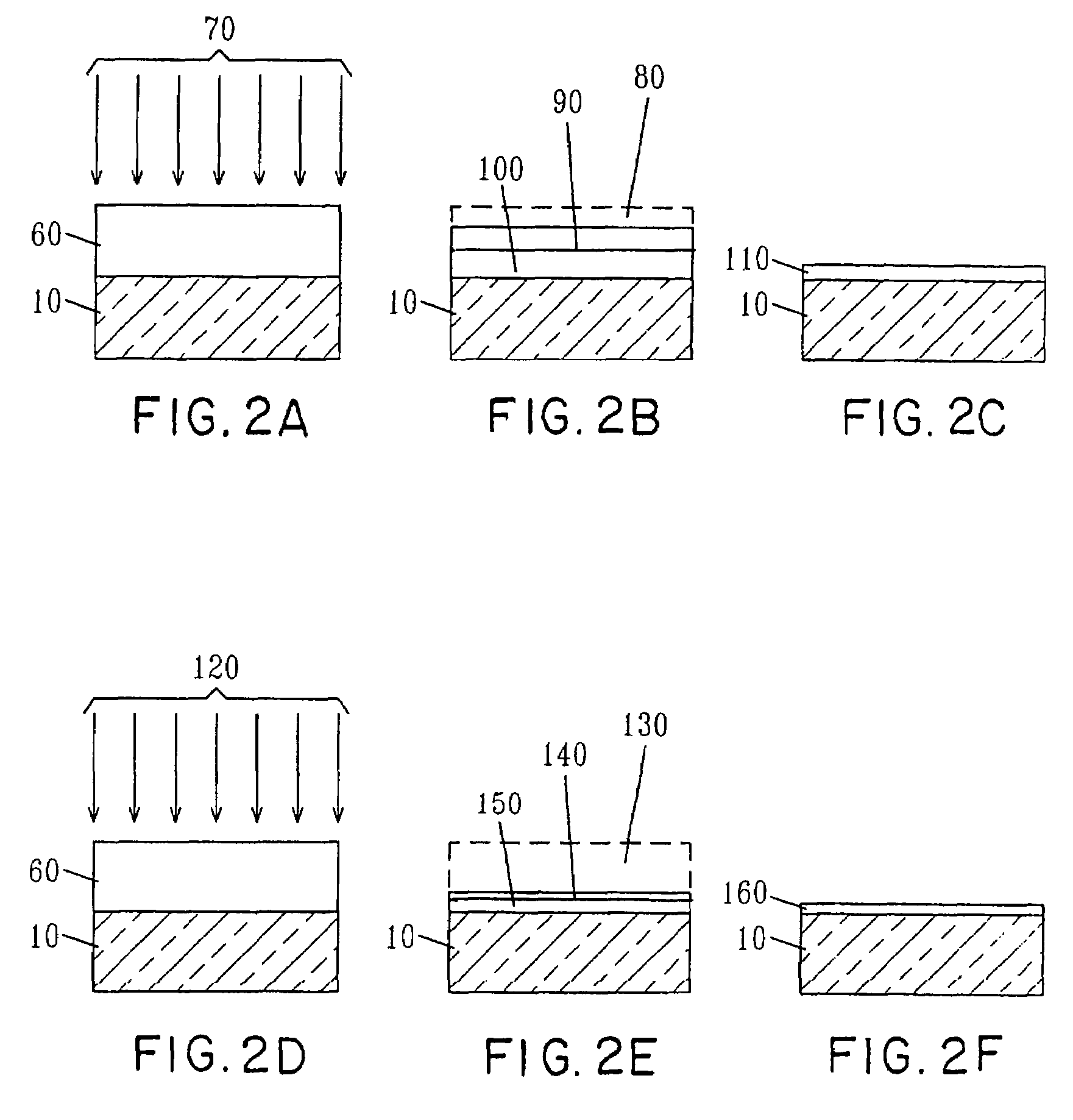
A method for making an ultrathin high-k gate dielectric for use in a field effect transistor is provided. The method involves depositing a high-k gate dielectric material on a substrate and forming an ultrathin high-k dielectric by performing a thinning process on the high-k gate dielectric material. The process used to thin the high-k dielectric material can include at least one of any number of processes including wet etching, dry etching (including gas cluster ion beam (GCIB) processing), and hybrid damage / wet etching. In addition to the above, the present invention relates to an ultrathin high-k gate dielectric made for use in a field-effect transistor made by the above method.

Description

FIELD OF THE INVENTION[0001]This invention generally relates to field effect transistors (FETs) and complementary metal oxide semiconductor (CMOS) devices incorporating high-k gate dielectrics. More particularly, it relates to FETs having ultrathin high-k gate dielectrics formed by etching back or thinning a thicker high-k dielectric film, and to methods for making FETs with these etched-back gate dielectrics.BACKGROUND OF THE INVENTION[0002]Performance improvements in field effect transistors (FETs) are typically effected by shrinking the FET dimensions, a design approach known as scaling. As scaling drives gate dielectric dimensions to ever-thinner equivalent oxide thicknesses (EOTs), high dielectric constant (high-k) metal oxides and metal silicates are becoming increasingly attractive as candidate gate dielectric materials. The higher k of these materials (compared to SiO2) allows them to have a thicker physical thickness for a given EOT, thus decreasing device leakage and impro...

Claims


Application Information

Patent Timeline
Patent Type & Authority Patents(United States)
IPC IPC(8): H01L21/31H01L21/28H01L21/283H01L21/311H01L21/314H01L21/336H01L21/8238H01L29/51H01L29/94
CPCH01L21/28194H01L21/31105H01L29/517H01L21/31122H01L21/31111
Inventor SAENGER, KATHERINE L.JAMMY, RAJARAONARAYANAN, VIJAY
Owner GLOBALFOUNDRIES US INC
Why Eureka
Try Eureka