Method of forming three-dimensional nanocrystal array

a nanocrystal array and three-dimensional technology, applied in the direction of nanoinformatics, polycrystalline material growth, crystal growth process, etc., can solve the problems of expensive lithography, non-trivial task of creating nanometer-size catalyst particles, and inability to meet the requirements of nanocrystal structure,

Inactive Publication Date: 2004-04-29
HEWLETT PACKARD DEV CO LP
View PDF3 Cites 99 Cited by
  • Summary
  • Abstract
  • Description
  • Claims
  • Application Information

AI Technical Summary

Problems solved by technology

However, creation of nanometer-size catalyst particles is a non-trivial task.
Although they can be registered to previously formed patterns, creating these patterns requires additional processing, usually involving costly lithography.
In addition, conventional lithography processes cannot readily form nanoparticles of the desired small dimensions.

Method used


Image

  • Method of forming three-dimensional nanocrystal array
  • Method of forming three-dimensional nanocrystal array
  • Method of forming three-dimensional nanocrystal array

Examples


Embodiment Construction

[0026] Reference is made now in detail to specific embodiments, which illustrate the best modes presently contemplated by the inventors. Alternative embodiments are also briefly described as applicable.

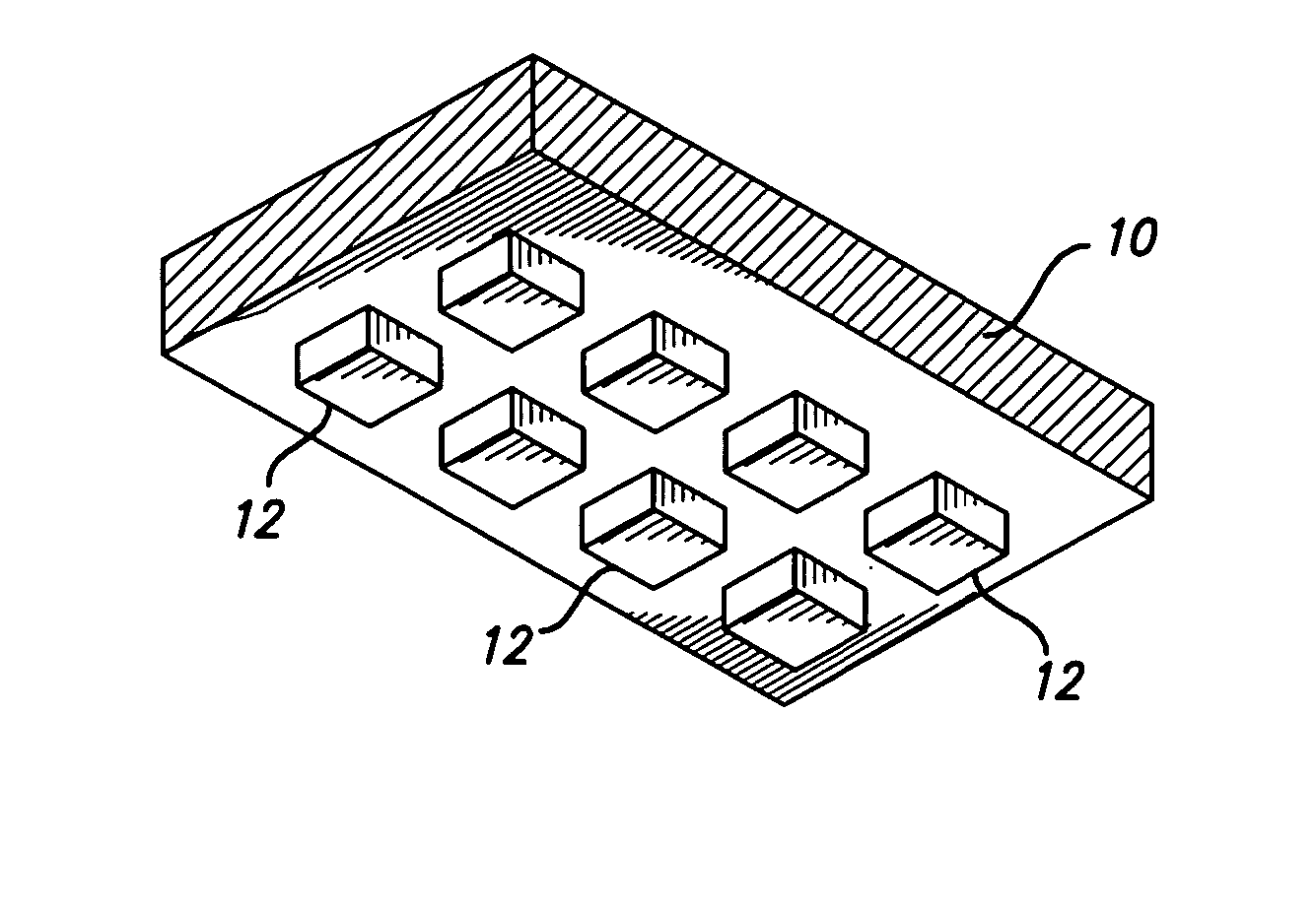
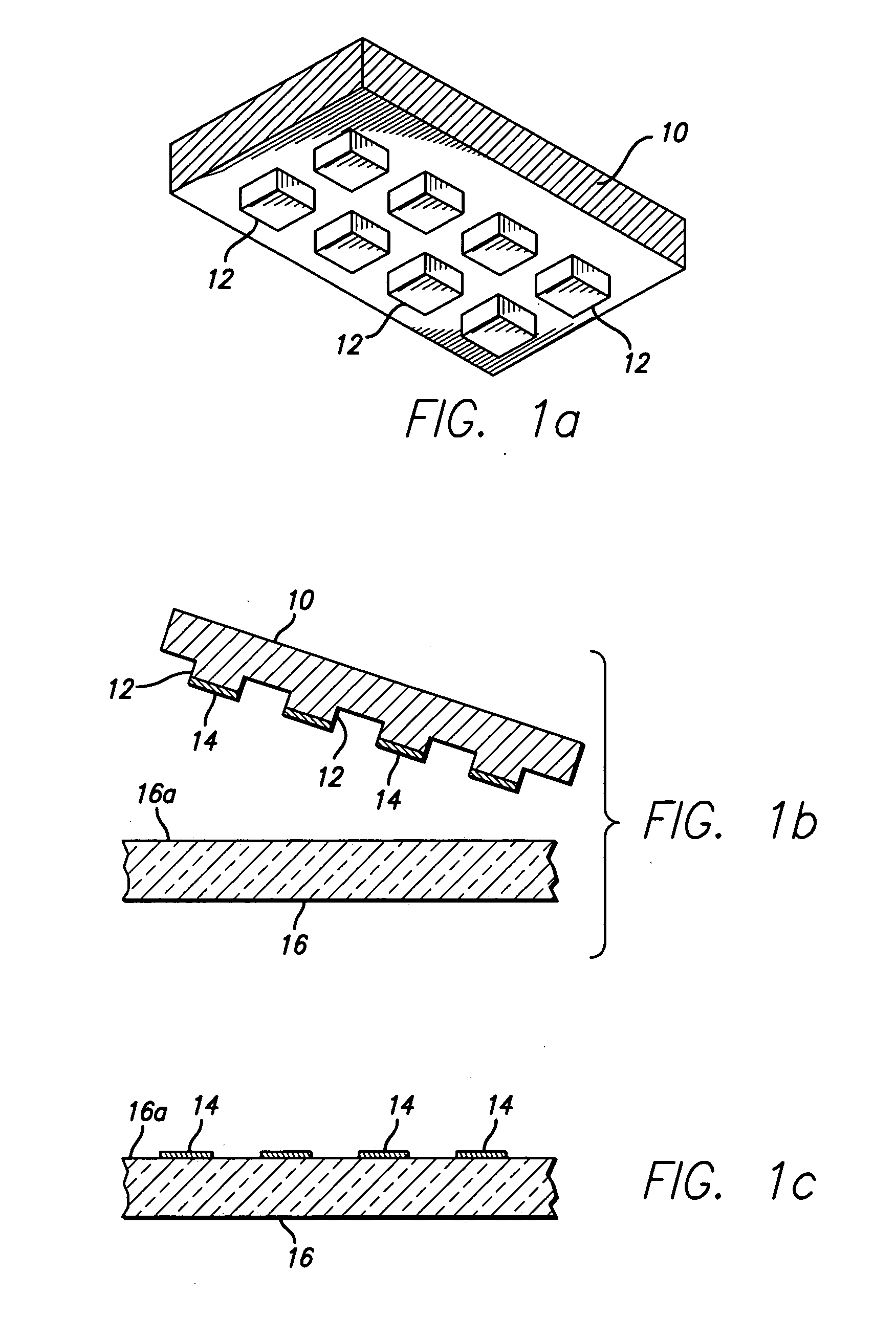
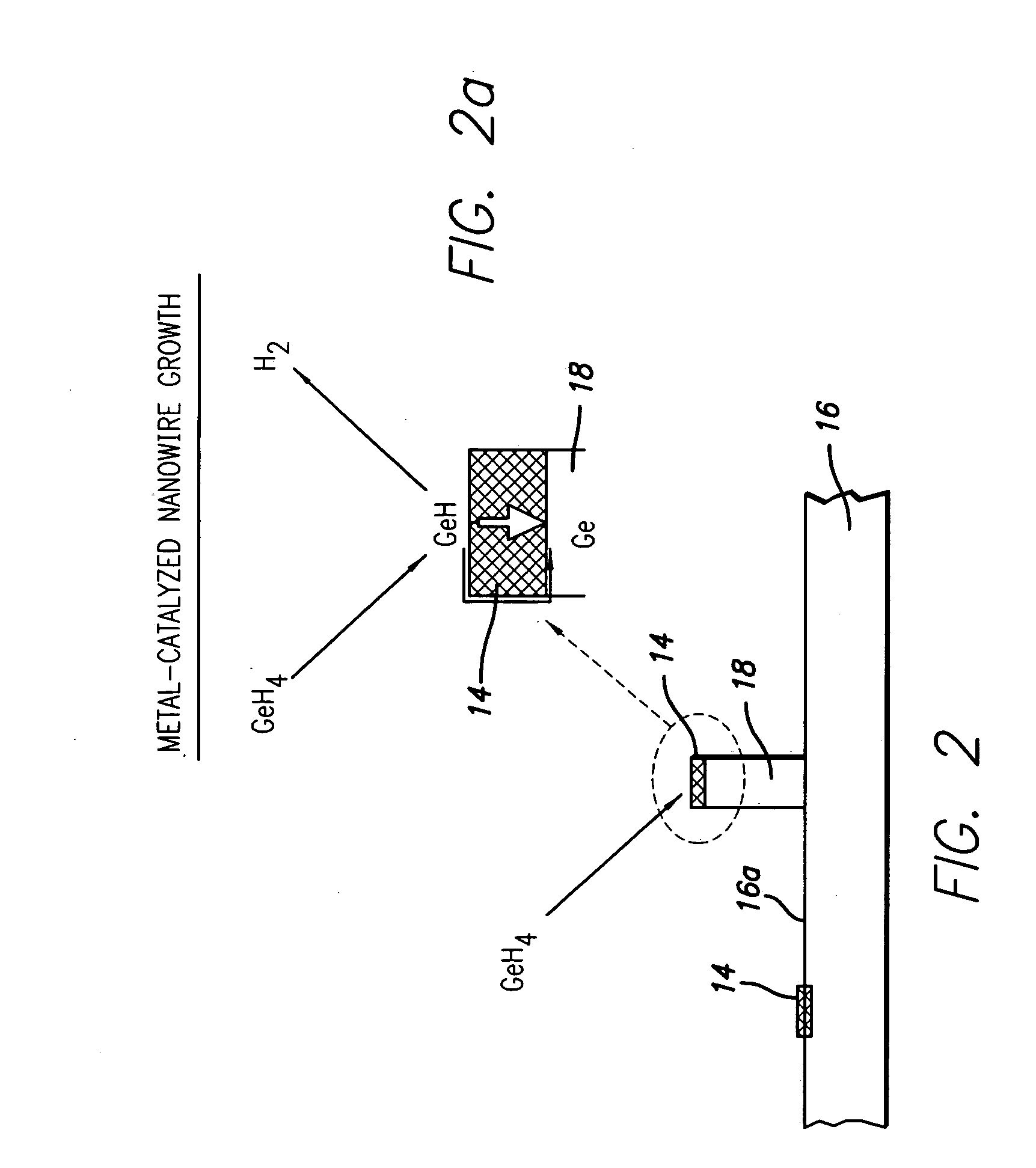
[0027] In accordance with the teachings herein, the composition of nanowires can be changed during growth so that different materials are at different positions along the length of the nanowire. This permits forming alternating regions of Si and Ge. If the nanowires are in an ordered array, for example, nucleated by the array formed by the method of the above-referenced patent application, then a three-dimensional array of nanocrystals can be formed by varying the composition of each wire in the array along its length. For the example of Si and Ge, three-dimensional nanocrystalline arrays of Si and of Ge may be formed, with the elements of each array bounded on top and bottom by the other element and the sides bounded by the gap between the nanowires.

[0028] In accordance with one embo...


PUM

PropertyMeasurementUnit
lateral sizeaaaaaaaaaa
depthaaaaaaaaaa
diameteraaaaaaaaaa

Abstract

A method of forming an assembly of isolated nanowires of at least one material within a matrix of another material is provided. The method comprises: providing a substrate; forming a catalyst array on a major surface of the substrate; growing an array of the nanowires corresponding with the catalyst array, the nanowires, each comprising at least one material; and forming a matrix of another material that fills in spaces between the nanowires. The method is useful for producing a variety of structures useful in a number of devices, such as photonic bandgap structures and quantum dot structures.

Description

[0001] The present application is a continuation-in-part application of application Ser. No. 10 / 281,678, filed Oct. 28, 2002, entitled "A Method of Forming Catalyst Nanoparticles for Nanowire Growth and Other Applications", filed in the names of Theodore I. Kamins et al and assigned to the same assignee as the present application. That application is directed to the growth of silicon nanowires for forming arrays of such nanowires having a large surface-to-volume ratio. The techniques disclosed therein are employed in the practice of the present embodiments.[0003] The present invention is directed to the fabrication of a plurality of single-material or segmented nanowires embedded in a matrix.[0004] Bulk synthesis of semiconductor wires has been traditionally achieved using several variations of metal catalyzed techniques, such as vapor-liquid-solid (VLS) synthesis. In conventional metal-catalyzed nanowire synthesis techniques used for producing semiconductor (e.g., silicon) nanowire...

Claims


Application Information

Patent Timeline
Patent Type & Authority Applications(United States)
IPC IPC(8): C30B11/00C30B11/12
CPCB82Y10/00B82Y30/00C30B11/00C30B11/12H01L2924/0002C30B29/605H01L2924/00B82B3/00C30B23/00
Inventor KAMINS, THEODORE I.KUEKES, PHILIP J.
Owner HEWLETT PACKARD DEV CO LP
Why Eureka
Try Eureka