Semiconductor memory device having hierarchical structure of data input/output line and precharge method thereof

a memory device and data input/output technology, applied in the field of semiconductor memory devices, can solve the problems of data input/output control apparatus having such a conventional hierarchical structure and having a disadvantage of increasing the write-read cycle tim

Active Publication Date: 2004-05-06
SAMSUNG ELECTRONICS CO LTD
View PDF4 Cites 37 Cited by
  • Summary
  • Abstract
  • Description
  • Claims
  • Application Information

AI Technical Summary

Problems solved by technology

As shown in FIG. 2, the data input/output control apparatus having such a conventional hierarchical structure has a disadvantage o...

Method used


Image

  • Semiconductor memory device having hierarchical structure of data input/output line and precharge method thereof
  • Semiconductor memory device having hierarchical structure of data input/output line and precharge method thereof
  • Semiconductor memory device having hierarchical structure of data input/output line and precharge method thereof

Examples


Embodiment Construction

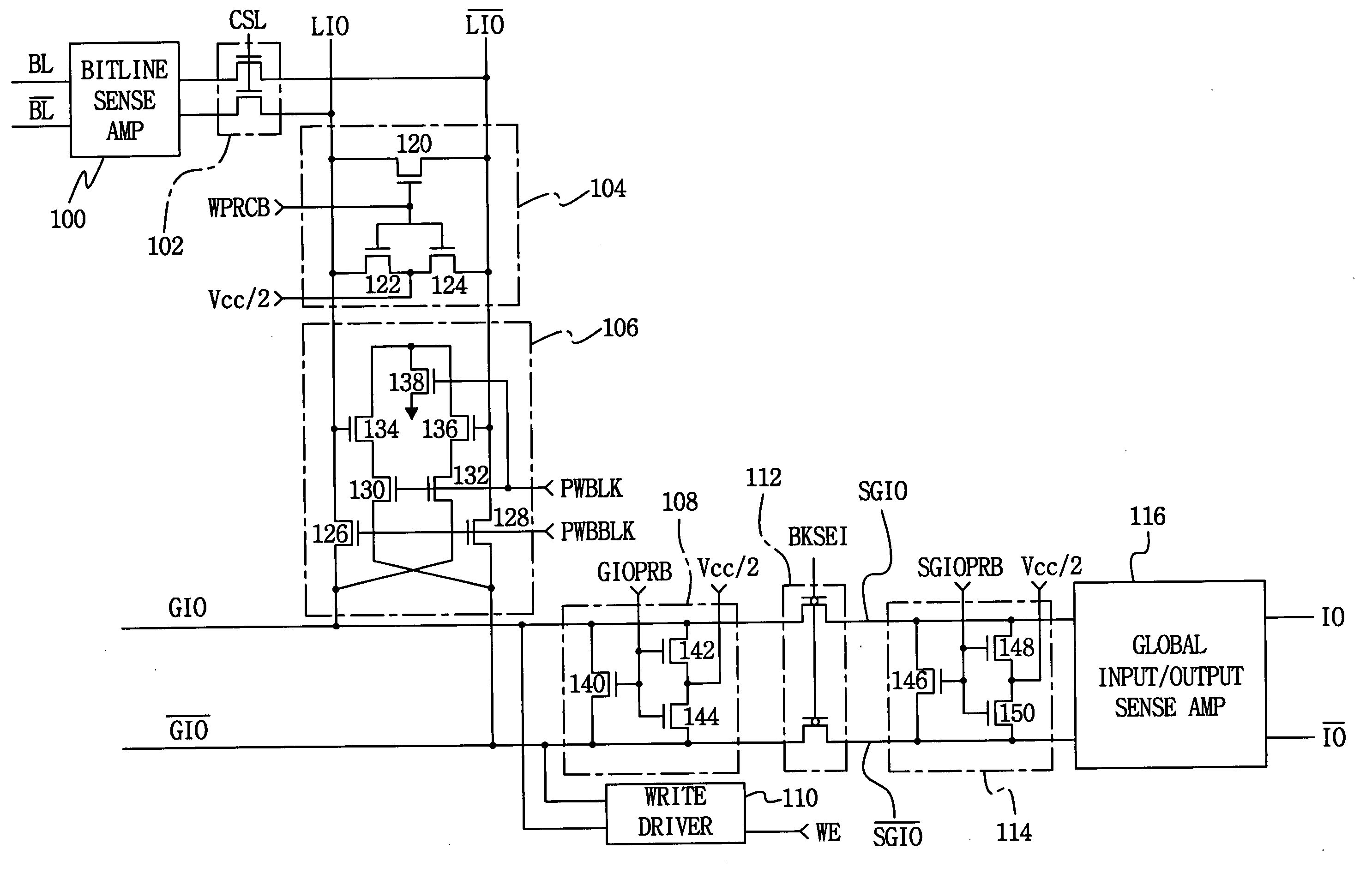
[0031] The present invention and exemplary embodiments thereof are more fully described below with reference to the accompanying drawings. This invention may, however, be embodied in many different forms and should not be construed as being limited to the exemplary embodiments set forth herein; rather, these exemplary embodiments are provided so that this disclosure is thorough and complete, and conveys the concept of the invention to those skilled in the art. In the inventive description, details of widely known functions of constructions will be omitted for the sake of brevity.

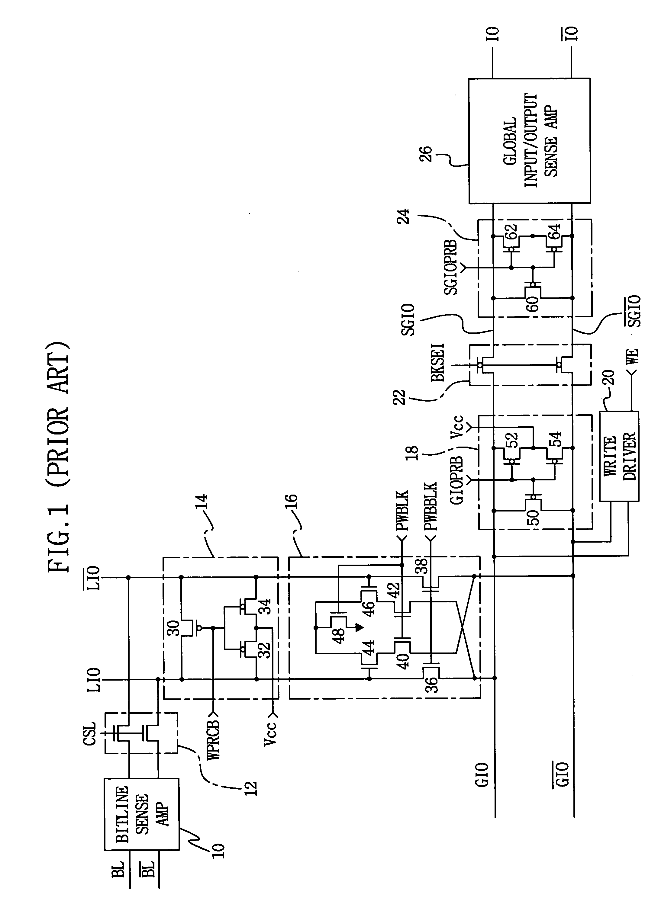
[0032] In a semiconductor memory device having a hierarchical structure, a precharge method of a data input / output apparatus is provided in such a structure that one pair of bitlines BL, / BL is connected to one pair of local input / output lines LIO, / LIO, and the one pair of local input / output lines LIO, / LIO is connected to one pair of global input / output lines GIO, / GIO.

[0033] FIG. 3 is a circuit diagram illu...


PUM


Abstract

A semiconductor memory device having a hierarchical structure of data input/output lines and a precharge method thereof. A precharge method in a semiconductor memory device having a hierarchical structure includes precharging the global input/output line pairs with half of a memory cell array voltage, and precharging the local input/output line pairs with the half of the memory cell array voltage.

Description

[0001] This U.S. nonprovisional patent application claims priority under 35 U.S.C. .sctn.119 of Korean Patent Application 2002-67405 filed on Nov. 01, 2002, the entire contents of which is hereby incorporated by reference.FIELD OF THE INVENITON[0002] The present invention relates to a semiconductor memory device, and more particularly, to a precharge method of precharging a local input / output line and a global input / output line in a semiconductor memory device with data input / output lines havinga hierarchical structure.DESCRIPTION OF THE RELATED ART[0003] A semiconductor memory device generally employs a sense amplifier for sensing data of each cell. To speed up an operation of the sense amplifier, the sense amplifier may be equalized. Techniques for equalizing a sense amplifier are disclosed in the U.S. Pat. No. 4,962,324 published on Oct. 09, 1990. U.S. Pat. No. 4,962,324 discloses a sense amplifier equalizing circuit that is resistant against Vcc or Vss noise, in which a sufficie...

Claims


Application Information

Patent Timeline
IPC IPC(8): G11C7/10G11C7/00
CPCG11C7/10G11C7/1048G11C7/1051G11C2207/002G11C7/1078G11C7/1096G11C7/1069G11C7/00
Inventor LIM, KYU-NAMKYUNG, KYE HYUN
Owner SAMSUNG ELECTRONICS CO LTD
Why Eureka
Try Eureka