

Novel field effect transistor and method of fabrication
a transistor and new technology, applied in the field of depleted substrate transistors, can solve the problems of gate length scaling and gate oxide scaling that can be reliably and uniformly achieved with today's structures and processes, and achieve the effect of increasing the amount of gate oxide scaling and gate length scaling
- Summary
- Abstract
- Description
- Claims
- Application Information
AI Technical Summary
Problems solved by technology
Method used
Image

Examples
Embodiment Construction
[0009] The present invention is a novel field effect transistor and its method of fabrication. In the following description numerous specific details have been set forth in order to provide a thorough understanding of the present invention. However, one of ordinary skill in the art, will realize that the invention may be practiced without these particular details. In other instances, well-known semiconductor equipment and processes have not been described in particular detail so as to avoid unnecessarily obscuring the present invention.
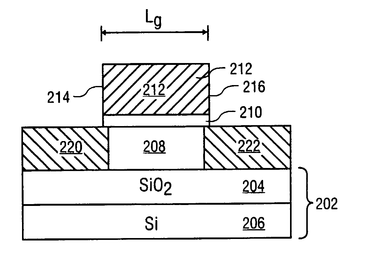
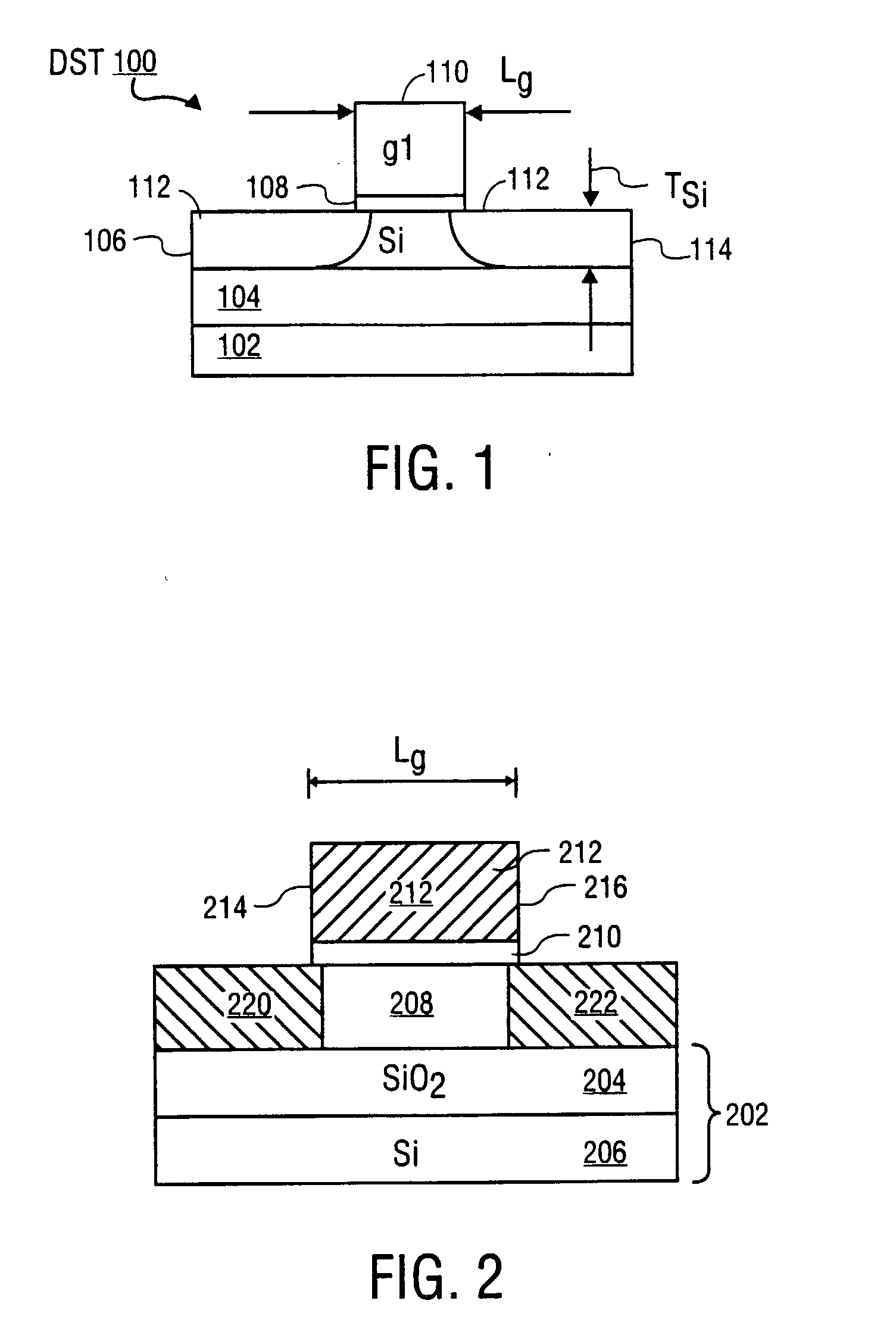
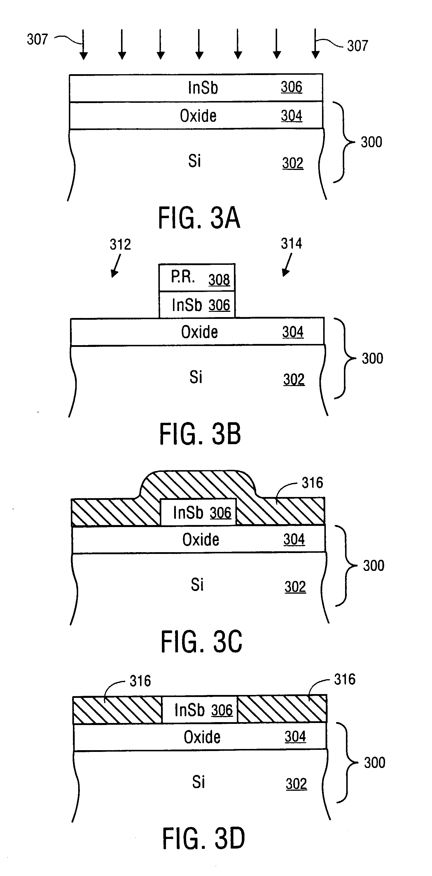
[0010] The present invention is a novel field effect transistor and its method of fabrication. The transistor of the present invention has an ultra high channel mobility formed from a narrow bandgap semiconductor, such as InSb. Because a channel is formed from a narrow bandgap material (less than 0.7 eV at room temperature) it has a high channel mobility and saturation velocity which results in more drive current for lower voltages. Large drive curren...
PUM
 Abstract
Description
Claims
Application Information