Stacked variable inductor

a variable inductor and inductor technology, applied in the direction of inductance, inductance, discontinuously variable inductance/transformer, etc., can solve the problems of inability to use inductor above the resonance frequency, inability to vary the impedance, and the complexity of the rf blocks of recent rf ic technology

Active Publication Date: 2004-07-22
ELECTRONICS & TELECOMM RES INST
View PDF4 Cites 139 Cited by
  • Summary
  • Abstract
  • Description
  • Claims
  • Application Information

AI Technical Summary

Problems solved by technology

RF blocks of recent RF IC technology has become more complicated to accommodate various services such as 900 MHz cellular, 1.5 GHz GPS, 1.9 GHz PCS, 2.4 GHz Blue-tooth, 5.2 GHz WLAN.
However, this variable inductor has disadvantage that parasitic capacitance presenting between stacked inductors causes a resonance frequency f.sub.res low to be 0.9.about.1.8 GHz so that the inductor can not be used above the resonance frequency and it's impedance can not be varied.
This inductor is formed with single layer and occupies large area, so that it's impedance cannot be variably used.
However, additional power consumption is required for the inductor and the inductor cannot be applied for frequency above 1.about.2 GHz.

Method used


Image

  • Stacked variable inductor
  • Stacked variable inductor
  • Stacked variable inductor

Examples


first embodiment

[0031] (First Embodiment)

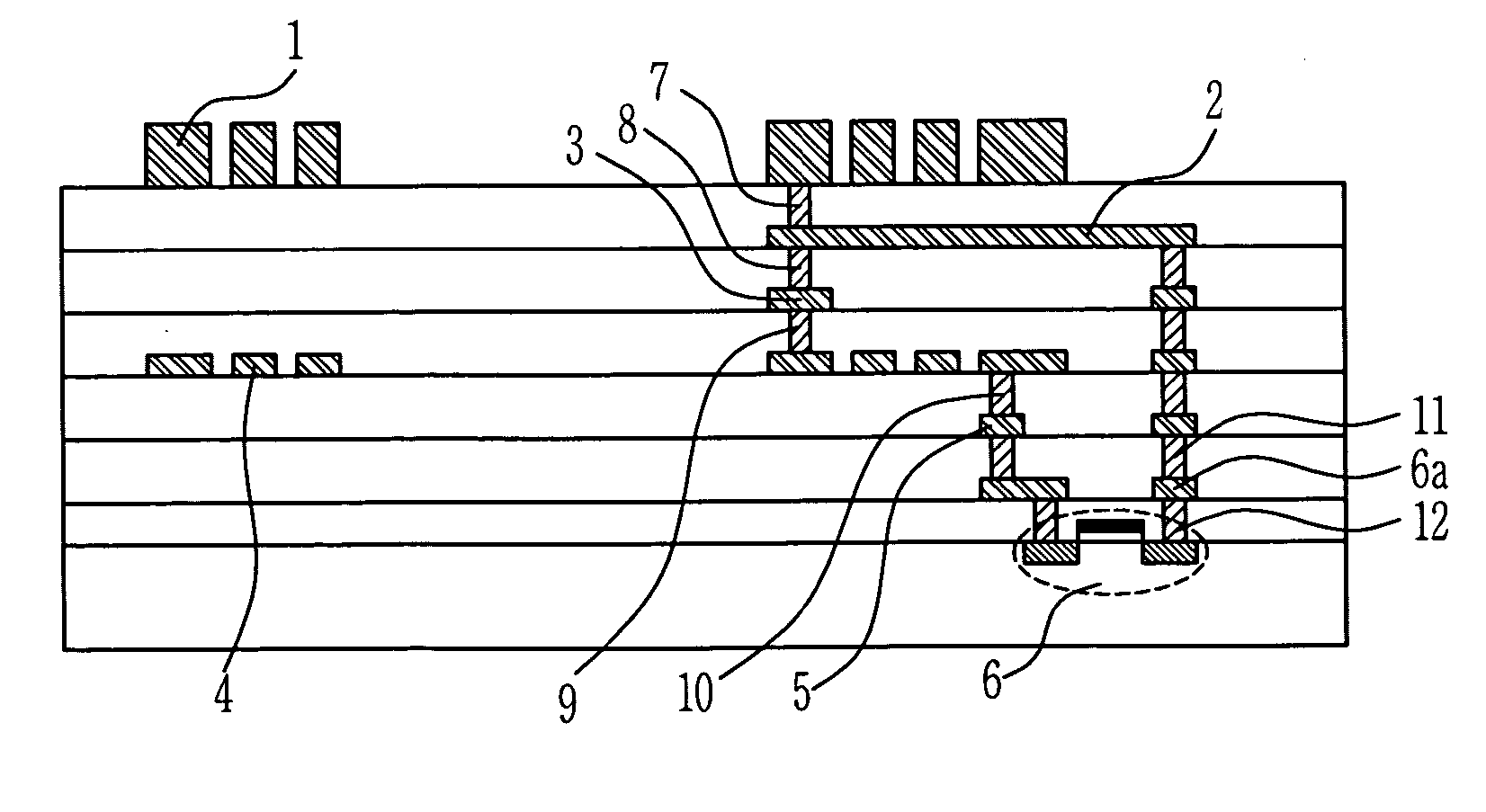
[0032] Hereinafter, the integrated variable inductor in accordance with the first embodiment of the present invention will be explained in detail with reference to FIGS. 4 and 5. FIG. 4 is a concept view for explaining a stacked variable inductor in accordance with a first embodiment of the present invention, and FIG. 5 shows a cross sectional view that is applied to actual substrate by using CMOS technology in accordance with the first embodiment of the present invention.

[0033] Referring to FIG. 4, a switching element 6 is connected between stacked upper inductor and lower inductor L1 and L2 using CMOS technology that have different values of inductance when the element is turned on / off, thereby the variable inductor can be implemented as single stacked inductor. One terminal of each of upper and lower inductors L1 and L2 is connected to the port 1 or port 2, and the other one of each of upper and lower inductors L1 and L2 is connected each other by contact...

second embodiment

[0042] (Second Embodiment)

[0043] Hereinafter, an integrated variable inductor in accordance with the second embodiment of the present invention will be explained with reference to FIG. 7. Difference between the first and second embodiments can be described for the number of turns of inductor L1 and L2.

[0044] In the second embodiment, the variable inductance range of one inductor can be increased from adjustment of turns of each inductor. Alternatively, when the transistor is turned on, total inductance has an inductance value of L1 if the transistor is an ideal switch. But, there exists a resistance R.sub.on of the transistor, so the number of L2 turns can be increased in order to increase the impedance of the inductor L2 higher than impedance of the transistor while the transistor is On state.

third embodiment

[0045] Third Embodiment

[0046] Hereinafter, a stacked variable inductor using three inductors 35, 37, and 38 each formed on a different layer in accordance with the third embodiment of the present invention will be explained with reference to FIG. 8. For example, inductors are formed by metal layers each on sixth, fourth, and second layers, and a first switching element 39 is connected between a terminal 36 and a port 2, and a second switching element 40 is connected between a port 2 and a terminal between the inductor 37 and inductor 38.

[0047] In this embodiment, the inductance can be varied to three values in accordance with the ON / OFF states of switches S1 39 and S2 40. It is also understood that R.sub.on and C.sub.off when the switch is turned on / off should be taken into consideration as is described in the above embodiments.


PUM

PropertyMeasurementUnit
operation frequencyaaaaaaaaaa
carrier frequencyaaaaaaaaaa

Abstract

Disclosed is a stacked variable inductors manufactured by stacking M (M>=2) metal layers on a semiconductor substrate, and provides stacked variable inductors comprising, 1 to N inductors continuously connected in serial, wherein each of said inductors is formed on N (N<=M) metal layers that are different each other; first and second ports each connected to the highest positioned inductor and to the lowest positioned inductor among said 1 to N inductors; and at least one MOSFET, and wherein one terminal of at least one MOSFET is connected to one of the first and second ports, and the other one is connected to one of adjacent terminals connected in serial between 1 to N inductors.

Description

[0001] 1. Field of the Invention[0002] The present invention relates to a stacked variable inductor, in particular to the inductor that can have variable inductance by using MOSFETs and inductors formed on two or more than two different layers in a CMOS structure having a plurality of metal layers.[0003] 2. Description of the Prior Art[0004] RF blocks of recent RF IC technology has become more complicated to accommodate various services such as 900 MHz cellular, 1.5 GHz GPS, 1.9 GHz PCS, 2.4 GHz Blue-tooth, 5.2 GHz WLAN. This occurs because that a carrier frequency of each service is different so that transmitting / receiving circuit that is to be processed should be changed in accordance with each band of the carrier frequency. The most part that is changing from the transmitting / receiving circuit in accordance with a different carrier frequency is an impedance matching circuit.[0005] An inductance matching circuit usually consists of inductors and capacitors, and an integrated induc...

Claims


Application Information

Patent Timeline
Patent Type & Authority Applications(United States)
IPC IPC(8): H01L27/04H01F17/00H01F21/12H01L21/02H01L23/522
CPCH01F17/0013H01F21/12H01L23/5227H01L28/10H01L2924/0002H01L2924/3011H01L2924/00H01L27/04
Inventor KIM, CHEON SOOPARK, PIL JAEPARK, MUN YANGYU, HYUN KYU
Owner ELECTRONICS & TELECOMM RES INST
Why Eureka
Try Eureka