Voltage generating circuit, voltage generating device and semiconductor device using the same, and driving method thereof

a voltage generation circuit and voltage generation technology, applied in the direction of pulse technique, process and machine control, instruments, etc., can solve the problems of reducing the reliability, reducing the signal logic amplitude, and inefficiently providing two or more independent sources, so as to maintain stably the voltage rise

Active Publication Date: 2004-09-23
PANASONIC CORP
View PDF5 Cites 42 Cited by
  • Summary
  • Abstract
  • Description
  • Claims
  • Application Information

AI Technical Summary

Benefits of technology

0009] An object of the present invention is to provide a voltage generating circuit and a voltage generating device which can stably maintain a raised voltage over a long p

Problems solved by technology

This may lead to a reduced signal logic amplitude, and thus lowered reliability.
However, power to one system is preferably supplied from a single power source, because it is inefficient to provide two or more independent sources.
Therefore, the circuit has the problem that it is difficult to keep the voltage of the connecting node N103 at a raised voltage higher th

Method used


Image

  • Voltage generating circuit, voltage generating device and semiconductor device using the same, and driving method thereof
  • Voltage generating circuit, voltage generating device and semiconductor device using the same, and driving method thereof
  • Voltage generating circuit, voltage generating device and semiconductor device using the same, and driving method thereof

Examples


first embodiment

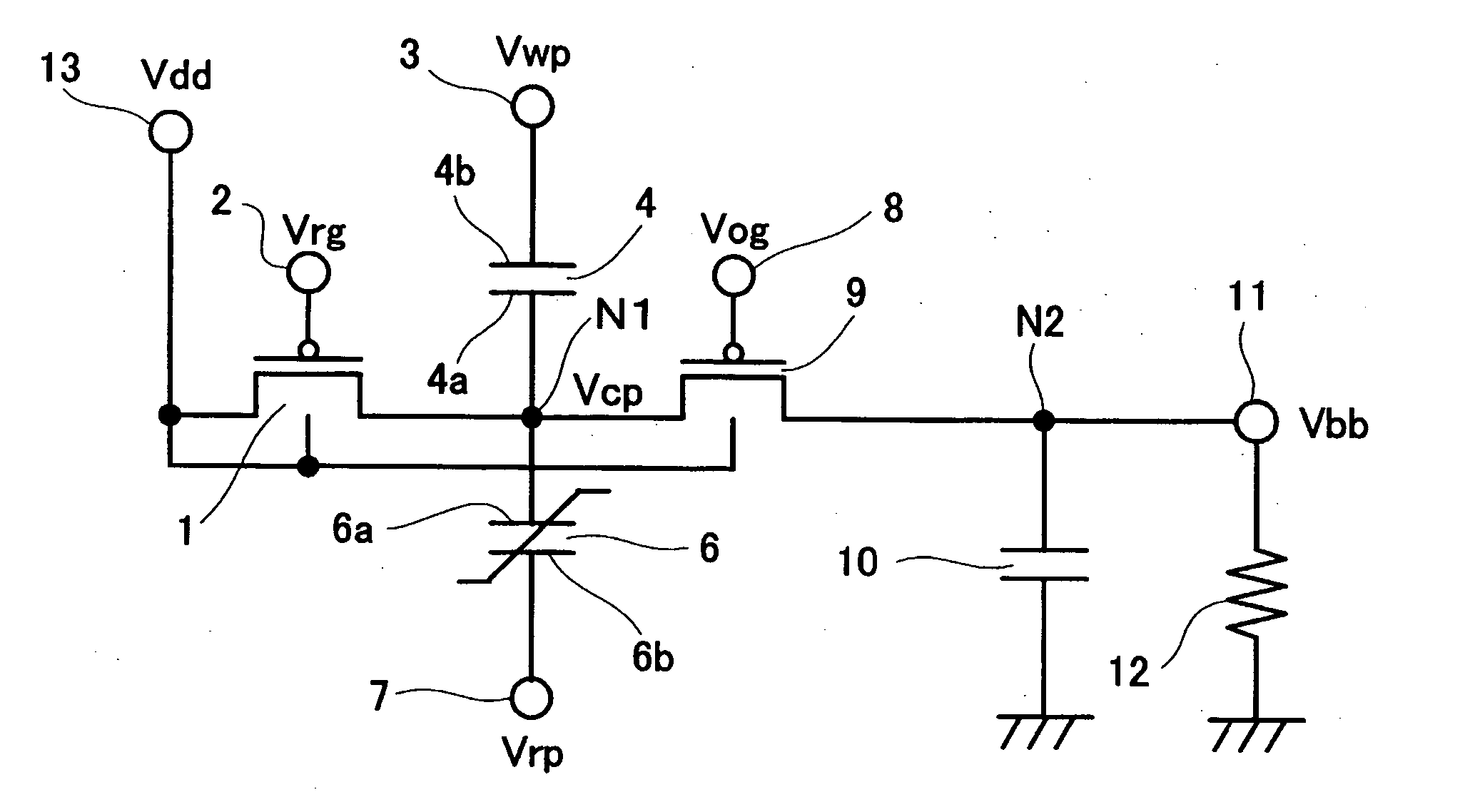
[0064] FIG. 3 is a time chart showing the change over time of the voltage applied to each terminal of the voltage generating circuit according to this FIG. 4 shows the rising characteristics of the output voltage Vbb outputted from the output terminal 11. FIGS. 5(a) and 5(b) are time charts which show the change of the output voltage Vbb and the voltage Vcp of the connecting node N1, respectively, in the voltage generating circuit according to this embodiment over the first through fourth periods. In FIGS. 3 and 5, t1 to t4 correspond to the first to fourth periods described above respectively. Examples of the operation of the voltage generating circuit according to this embodiment will be described below with reference to FIGS. 3-5.

[0065] While on standby, as shown in FIG. 3, the voltages Vwp, Vog, Vrp, and Vrg of the write terminal 3, output control terminal 8, reset terminal 7 and reset control terminal 2 respectively, are set to the supply voltage Vdd, for example, 1 V.

[0066] (...

second embodiment

[0080] (Second Embodiment)

[0081] FIG. 6 is a block diagram schematically showing the configuration of the voltage generating device according to the second embodiment of the present invention. This voltage generating device comprises a first control circuit 21, first voltage generating circuit 22, second control circuit 23 and second voltage generating circuit 24. Herein, the first and second voltage generating circuits 22 and 24 have the voltage raising function described in the first embodiment. The voltage generating device according to this embodiment is configured with the two voltage generating circuits 22 and 24 connected serially. The first control circuit 21 controls the voltages applied to the terminals 2, 3, 7 and 8 of the first generating circuit 22 and the second control circuit 23 controls the voltages applied to the terminals 2, 3, 7 and 8 of the second generating circuit 24, as described in the first embodiment (see FIGS. 1 and 3). The first voltage generating circui...

third embodiment

[0084] (Third Embodiment)

[0085] FIG. 7(a) is a block diagram schematically showing the configuration of a voltage generating device according to the third embodiment of the present invention. FIG. 7(b) shows the change over time of the output voltage. As shown in FIG. 7(a), the voltage generating device according to this embodiment comprises a voltage generating circuit 26 having the voltage raising function described in the first embodiment, a control circuit 25 for controlling the operation of the voltage generating circuit 26 and a voltage detection circuit 27 for detecting an output voltage Vbb outputted from the voltage generating circuit 26.

[0086] The control circuit 25 controls the voltages applied to the terminals 2, 3, 7 and 8, as described in the first embodiment (see FIGS. 1 and 3). The signal symbol .phi. shown in FIG. 7(a) represents the voltages Vrg, Vwp, Vrp and Vog applied to terminals 2, 3, 7 and 8 of the voltage generating circuit 26 respectively. The control circu...


PUM


Abstract

A voltage generating circuit comprising a capacitor (4), a ferroelectric capacitor (6) serially connected to the capacitor (4), an output terminal (11), a capacitor (10) which grounds the output terminal (11), a supply voltage supplying terminal (13), a switch (1) which connects the supply voltage supplying terminal (13) and the connecting node (N1) of the two capacitors (4, 6), and a switch (9) which connects the connecting node (N1) and output terminal (11); wherein during a first period, with the two switches (1) and (9) placed in the OFF state, a terminal (3) is grounded and a terminal (7) is provided with a supply voltage; wherein during a second period, the terminal (3) is provided with the supply voltage and the switch (9) is placed in the ON state; wherein during a third period, the switch (9) is placed in the OFF state, the switch (1) is placed in the ON state, and the terminal (7) is grounded; wherein during a fourth period, the terminal (7) is provided with the supply voltage; and wherein thereafter the first through fourth periods are repeated.

Description

[0001] (1) Field of the Invention[0002] The present invention relates to a voltage generating circuit and a voltage generating device which have the function of increasing an input voltage, a semiconductor device using the same, and a driving method thereof.[0003] (2) Description of the Related Art[0004] LSIs, which are constructed by integrating many MIS transistors, have been increasingly miniaturized in recent years. Miniaturization of MIS transistors has been progressing in close accordance with a scaling law. Because of this trend, gate oxide films are becoming ultrathin. Therefore, to prevent an increased leakage current passing through the gate oxide films, and to maintain reliability, a lower supply voltage is required. For example, according to a design rule that specifies a minimum gate length of 0.13 .mu.m, the gate oxide film thickness is as thin as 1.5 to 1.9 nm and the supply voltage is as low as 1.2 to 1.5 V. When the potential of the gate of an MIS transistor and tha...

Claims


Application Information

Patent Timeline
IPC IPC(8): H02M3/07G11C11/22G11C11/407G11C11/4074G11C11/408H03K17/296H03K17/687H03K19/00H03K19/0948H03K19/185
CPCG11C11/22G11C11/4087G11C11/4074
Inventor TOYODA, KENJIUEDA, MICHIHITOMORIMOTO, KIYOSHIMORITA, KIYOYUKI
Owner PANASONIC CORP
Why Eureka
Try Eureka