
CMP slurry for nitride and CMP method using the same

Inactive Publication Date: 2004-10-14
SK HYNIX INC
View PDF8 Cites 14 Cited by
  • Summary
  • Abstract
  • Description
  • Claims
  • Application Information

AI Technical Summary

Benefits of technology

0012] Accordingly, a CMP slurry for nitride having a high polishing selectivity to nitride is disclosed

Problems solved by technology

These features cannot be achieved with etchback processes.
The oxide film deteriorates in a succeeding photolithography or etching processes which makes it impossible to form a suitable barrier nitride film using to the CMP process.
Consequently, the oxide CMP slurry cannot be used to polish nitride films deposited on oxide film patterns.

Method used


Image

  • CMP slurry for nitride and CMP method using the same
  • CMP slurry for nitride and CMP method using the same
  • CMP slurry for nitride and CMP method using the same

Examples


examples 1-5

Preparation of CMP Slurry for Nitride

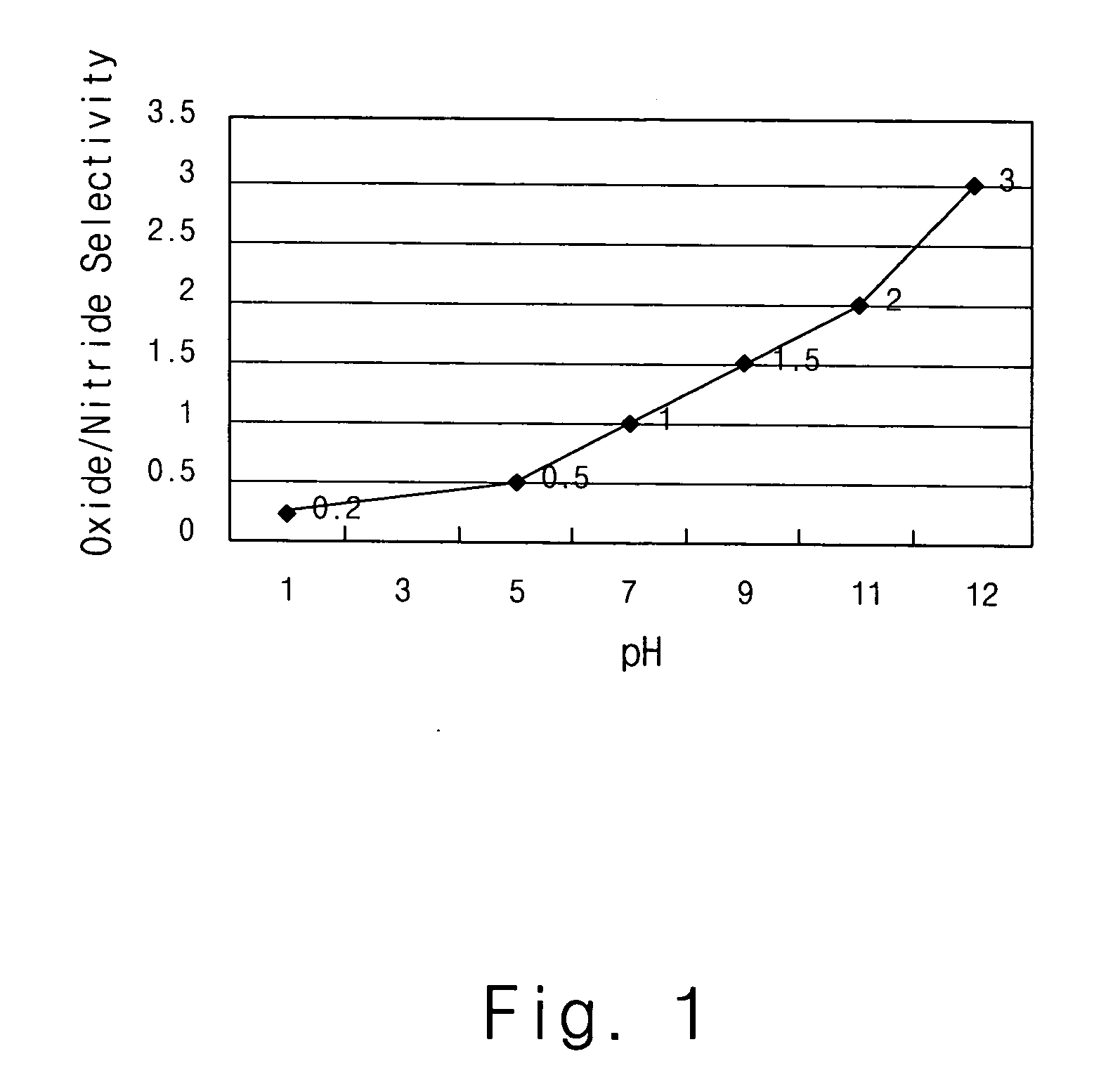
[0041] To 10 L deionized water was added a mixture acid of fluoric acid and nitric acid in a mixture ratio of 1:3 for fluoric acid:nitric acid. The mixture acid was added with 1 wt %, 0.75 wt %, 0.25 wt %, 0.08 wt % and 0.1 wt % of the gross slurry, thereby obtaining a CMP slurry having a pH shown in Table 1.

1 TABLE 1 Example 1 Example 2 Example 3 Example 4 Example 5 pH pH 1 pH 2 pH 3 pH 4 pH 5

examples 6-12

Preparation of CMP Slurry for Nitride

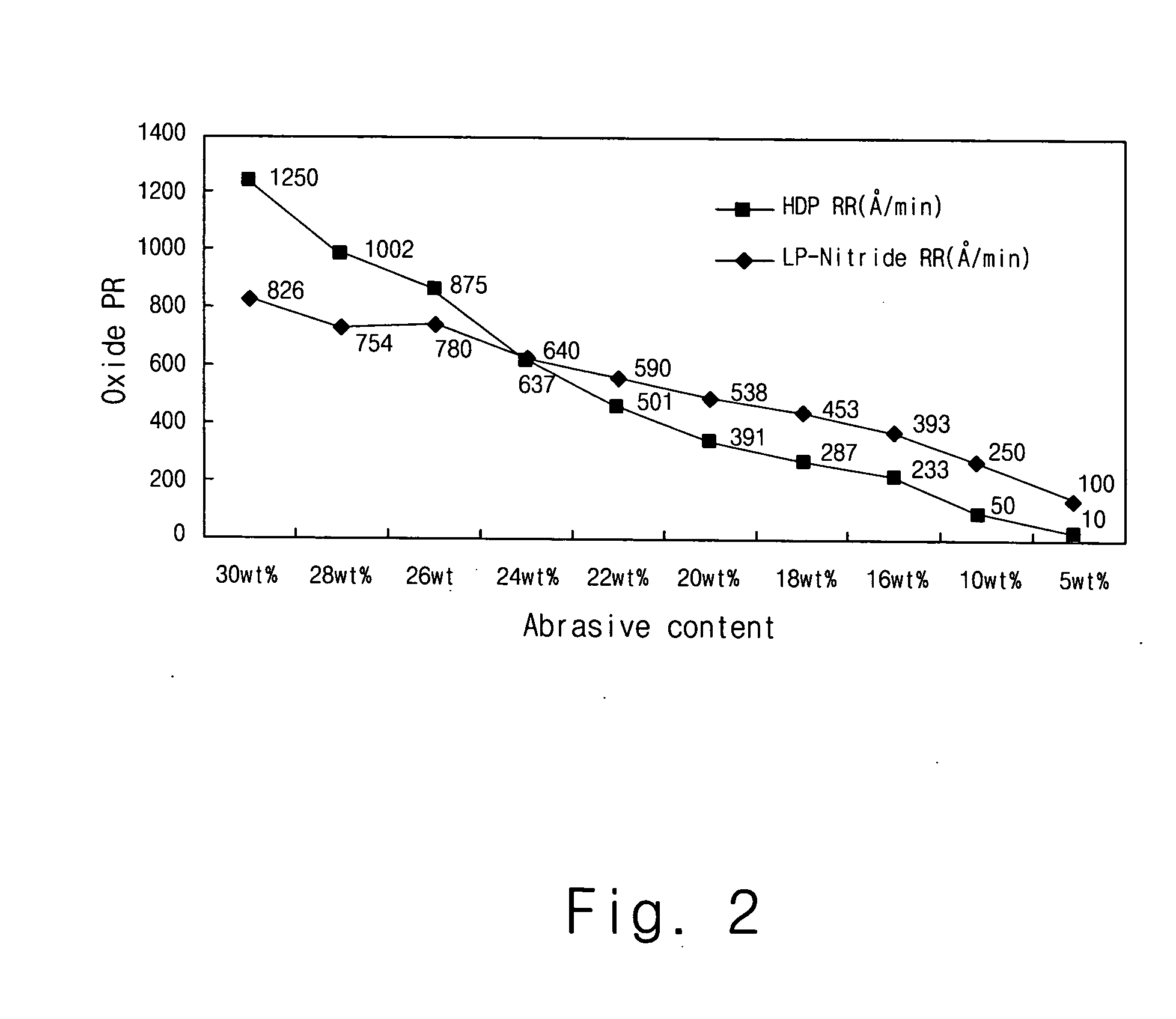
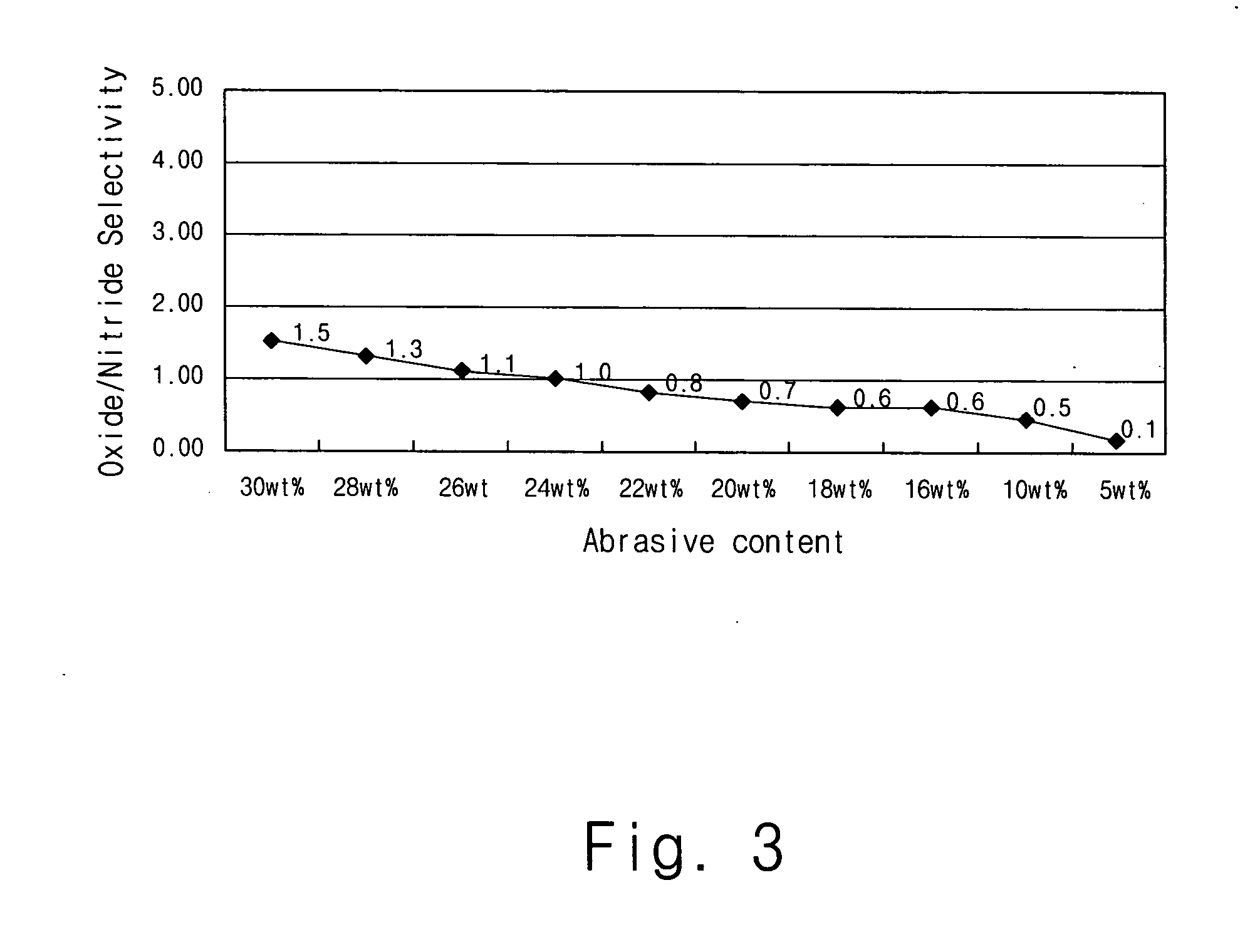
[0042] Deionized water was added to a CMP slurry containing a 30 wt % colloidal SiO.sub.2 abrasive, thereby obtaining a 10 L CMP slurry containing an abrasive to have a weight content of the gross slurry as shown in Table 2. Here, 1 wt % phosphoric acid was added so that the slurry may have a pH of 2.

2 TABLE 2 Exam- Exam- Exam- Exam- Exam- Exam-Exam- ple 6 ple 7 ple 8 ple 9 ple 10 ple 11 ple 12 wt % 24 wt % 22 wt % 20 wt % 18 wt % 16 wt % 10 wt % 5 wt %

examples 13-20

Preparation of CMP Slurry for Nitride

[0043] Deionized water was added to a CMP slurry containing a 30 wt % colloidal SiO.sub.2 abrasive, then the abrasive was present in an amount of 16 wt % of the gross slurry. Then, a phosphoric acid was added to the resulting solution, thereby obtaining a CMP slurry of Examples 13-20 having a pH as shown in Table 3.

3 TABLE 3 Ex- Ex- Ex- am- am- am-Exam- Exam- Exam- Exam- Exam- ple ple ple ple ple ple ple ple 13 14 15 16 17 18 18 20 pH 2.84 2.935 2.955 3 3.02 3.045 3.11 3.19


PUM


Abstract

Disclosed is a CMP slurry for nitride having a low selectivity to oxide. More specifically, a CMP slurry for nitride is disclosed which has a high selectivity to nitride by regulating a weight content of an abrasive and by varying a pH of the slurry in order to prevent the oxide from being polished faster than the nitride. As a result, a semiconductor device of high density and high integration can be manufactured.

Description

[0001] 1. Technical Field[0002] A slurry used in a chemical mechanical polishing (hereinafter "CMP") process is disclosed which is used in the manufacture of semiconductors. More specifically, a CMP slurry, that is used for polishing silicon nitride films such as SiN or SiON films, is disclosed, and a CMP method using the CMP slurry is also disclosed.[0003] 2. Description of the Related Art[0004] Recently, much interest has been focused on a method for forming fine patterns in a semiconductor manufacturing processes. Accordingly, there are strong demands for technology of planarizing unevenness on chip and wafer surface widely.[0005] The CMP process is one of the planarization technologies employed with lithography processes in the manufacturing of semiconductor devices. IBM developed the CMP process in late 1980's by combining a chemical removing process and a mechanical polishing process.[0006] As semiconductors are further miniaturized in the form of high density and multi-layer ...

Claims


Application Information

Patent Timeline
IPC IPC(8): B24B37/00C09G1/02C09K3/14H01L21/304H01L21/3105
CPCH01L21/31053C09G1/02C09K3/14
Inventor PARK, HYUNG SOON
Owner SK HYNIX INC
Learn More