

Cmp polishing agent, method for manufacturing thereof, and method for polishing substrate
- Summary
- Abstract
- Description
- Claims
- Application Information
AI Technical Summary
Benefits of technology
Problems solved by technology
Method used
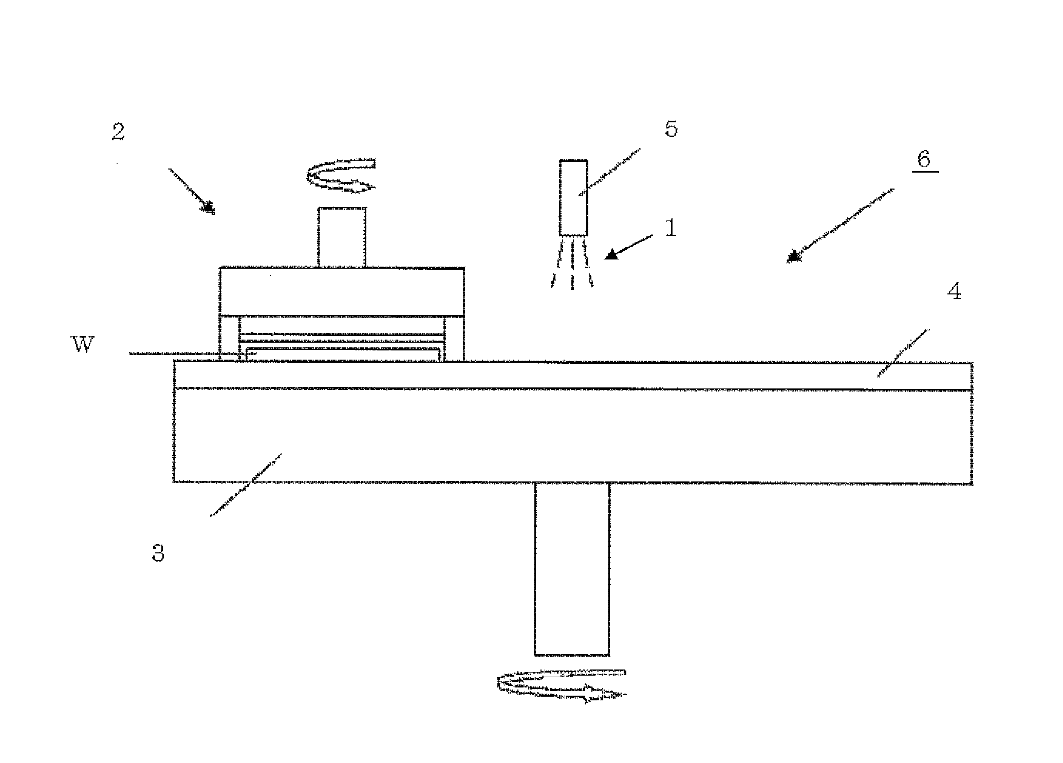
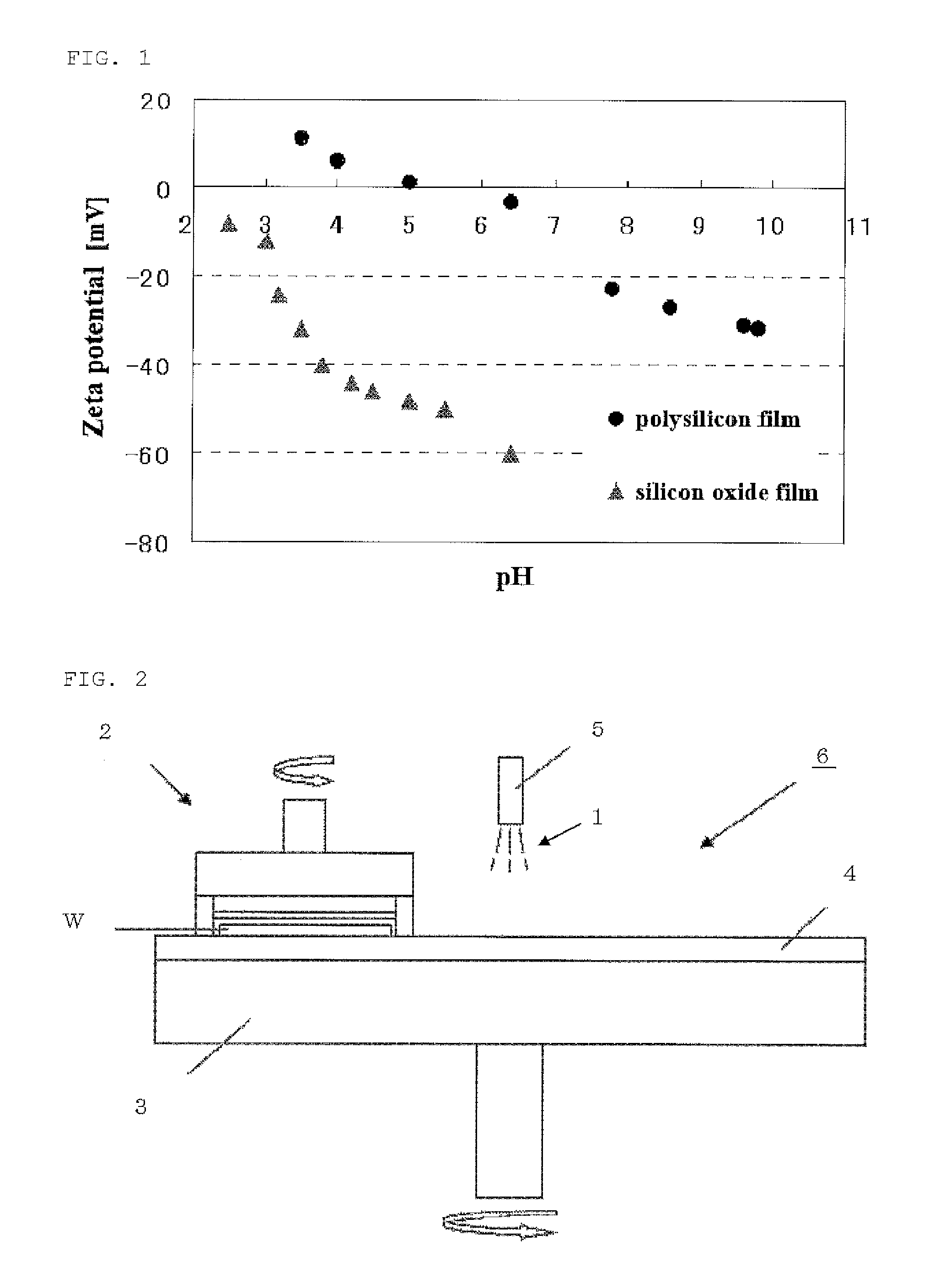
Image

Examples
example 1
[0098]A CMP polishing agent with the ceria particle concentration of 1 part by mass containing 0.15 part by mass of a copolymer of styrene and acrylonitrile was prepared as follows: 500 g of the wet ceria particles synthesized above, 15 g of a copolymer of styrene and acrylonitrile having an average molecular weight of 600, and 5000 g of pure water were mixed; subjected to ultrasonic dispersing for 60 minutes with stirring; then, filtered through a 0.5 micron filter; and diluted with pure water.
[0099]The pH of the obtained CMP polishing agent was 6.3. The distribution of particle diameters was measured with an ultrasonic attenuation particle size distribution analyzer (Zeta-APS: manufactured by Matec). As the result, the average particle size was 0.10 micrometer.
example 2
[0100]A CMP polishing agent was prepared in the same manner as in Example 1, except for adding a copolymer of styrene and acrylonitrile having an average molecular weight of 8000.
[0101]The pH of the obtained CMP polishing agent was 6.5. The distribution of particle diameters was measured with an ultrasonic attenuation particle size distribution analyzer (Zeta-APS: manufactured by Matec). As the result, the average particle size was 0.11 micrometer.
example 3
[0102]A CMP polishing agent was prepared in the same manner as in Example 1, except for adding a copolymer of styrene and acrylonitrile having an average molecular weight of 16000.
[0103]The pH of the obtained CMP polishing agent was 6.5. The distribution of particle diameters was measured with an ultrasonic attenuation particle size distribution analyzer (Zeta-APS: manufactured by Matec). As the result, the average particle size was 0.10 micrometer.
PUM
| Property | Measurement | Unit |
|---|---|---|
| Fraction | aaaaa | aaaaa |
| Percent by mass | aaaaa | aaaaa |
| Percent by mass | aaaaa | aaaaa |
Abstract
Description
Claims
Application Information