Method for manufacturing a polymer chip and an integrated mold for the same

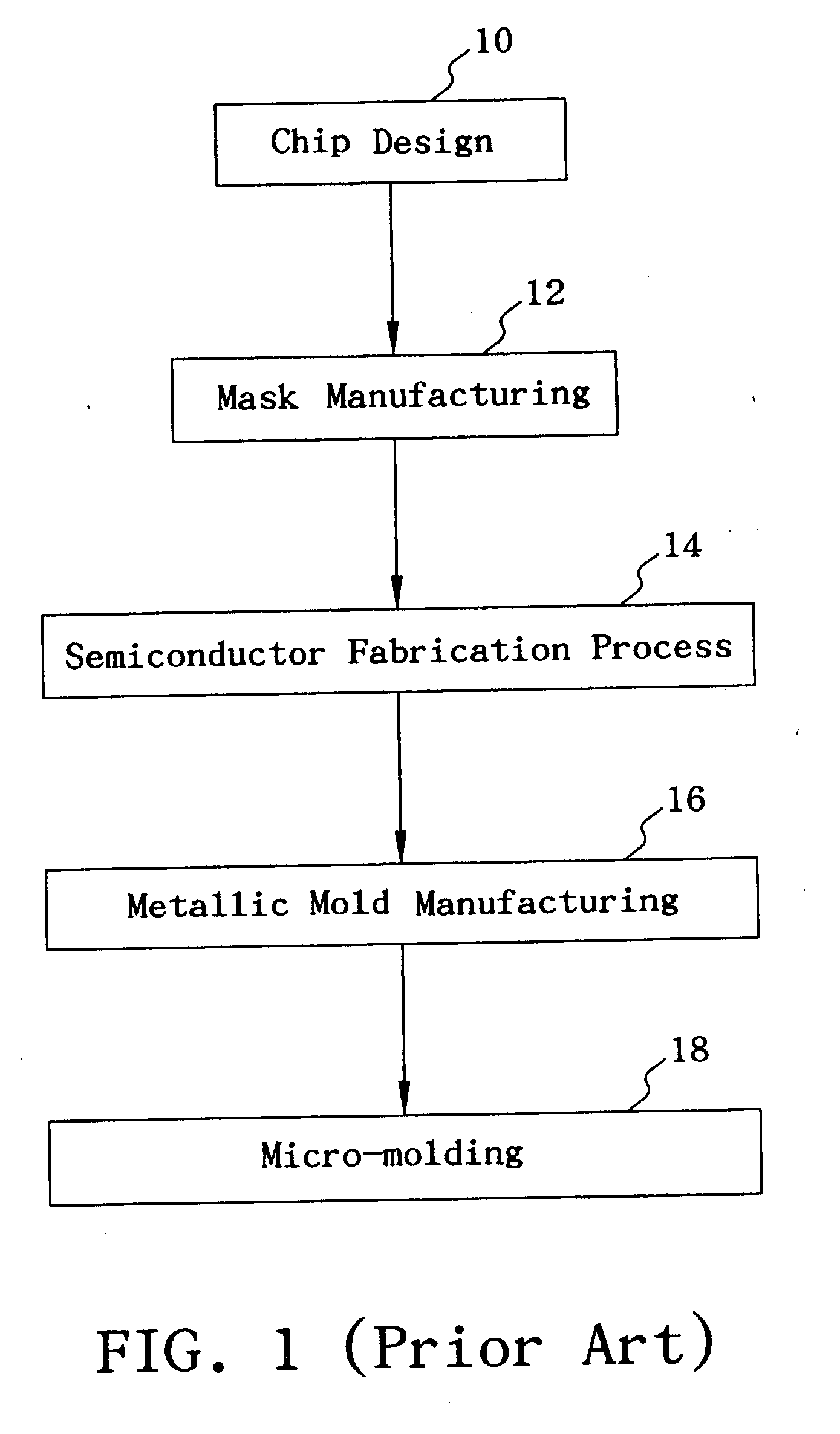
a polymer chip and mold technology, applied in semiconductor devices, solid-state devices, semiconductor/solid-state device details, etc., can solve the problems of high cost and time consumption of semiconductor fabrication processes, and the semiconductor fabrication process 14 is the most time-consuming and expensive step

Inactive Publication Date: 2004-11-04
IND TECH RES INST
View PDF20 Cites 36 Cited by
  • Summary
  • Abstract
  • Description
  • Claims
  • Application Information

AI Technical Summary

Problems solved by technology

The semiconductor fabrication process 14 in FIG. 1 could be very complicated and may involve a large number of sub-processes.
1. The semiconductor fabrication process is expensive and time-consuming:
In the steps shown in FIG. 1, mask manufacturing 12 and semiconductor fabrication process 14 are the most time-consuming and expensive steps.
Because these two steps use the professional techniques and equipments for the semiconductor fabrication, the manufacturing cost is rather expensive.
If the manufacturing is outsourcing, the schedule will be difficult to control.
Moreover, for a chip requiring small quantities and versatile types, the complicated semiconductor fabrication process will make the manufacturing cost for such small quantities and versatile types of chips even more expensive.
2. Lack of flexibility for changing the chip design
When there are design errors or impractical process in the manufacturing process of the chip and it is required to change the chip design, all the steps in FIG. 1 are necessary to be performed again, thus it is lack of flexibility for changing the chip design.
Thus, the flexibility for changing chip design is quite poor.
3. Practical semiconductor fabrication techniques are not available for chips comprising a number of zones among which specification of one zone is dramatically different from another.
50 .mu.m.times.50 .mu.m), poor quality may result from the conventional semiconductor process since only one set of process parameters can be used for both zones.
The parameters meeting the requirements for one zone may fail those for another zone.
The large difference in depth and width of the grooves on the same chip may generate a non-uniform surface.
Also, the interactive effect between processes performed on different zones of the chip will also make the manufacturing of chips more difficult.
For example, one zone on the chip may require high temperature etching or deposition processes while another zone not needing the processes may suffer from them if extra protection is not provided.
As the number of devices and functions integrated on the chip increases, the consideration by the interactive effect from various zones gets more complicated.
For the microfluidic chip being miniaturized, additional steps for the design and manufacturing of the second floor couplers could be an issue.
Besides, possibility of leakage at the coupler / module interfaces is another concern in such design.
In addition, tremendous alignment and bonding efforts necessary for the two-level multi-element assembly is another issue to be considered.

Method used


Image

  • Method for manufacturing a polymer chip and an integrated mold for the same
  • Method for manufacturing a polymer chip and an integrated mold for the same
  • Method for manufacturing a polymer chip and an integrated mold for the same

Examples


Embodiment Construction

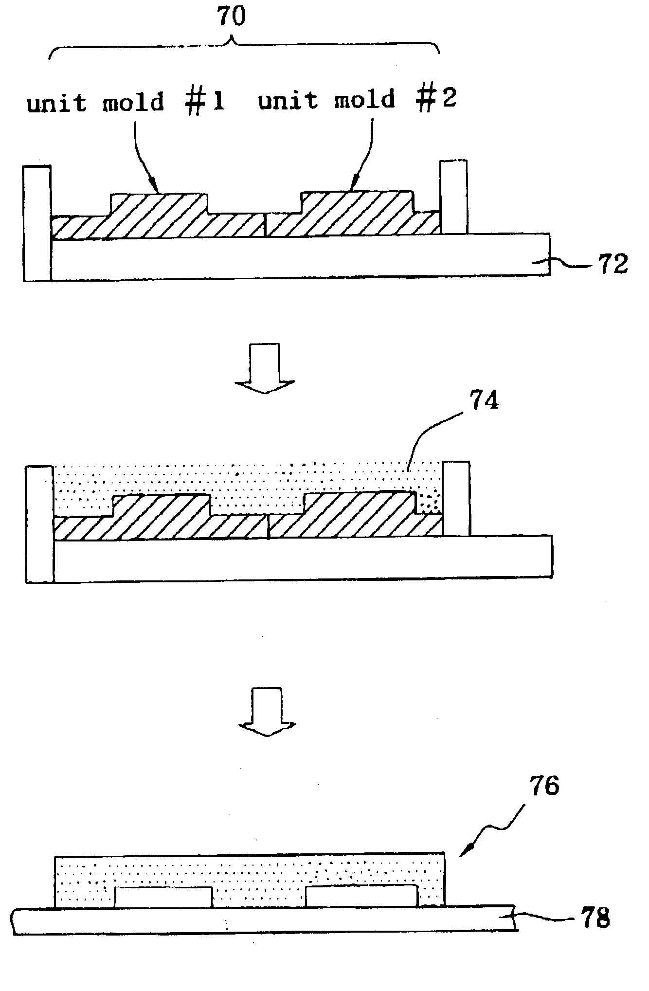
[0033] FIG. 3 shows a flow chart for manufacturing the polymer chip according to the present invention. As shown in FIG. 3, the present invention method for manufacturing the polymer chip mainly includes the chip design 20, manufacturing the unit molds 22, selecting / assembling the unit molds 24, and micro-molding of the polymer chips 26. The manufacturing of unit molds 22 can be performed in advance, for example, a series of commonly used unit molds such as channels, wells, mixers and T-shaped channels are manufactured in advance.

[0034] FIG. 4 illustrates a series of unit molds 30. The present invention analyzed the characteristics of the polymer chip, divided it into several classifications, and manufactured the unit molds 30. As shown in FIG. 4, the unit pattern 32 for the unit mold 30 may be a strip, a circle, or any other simple or complicated shapes. The patterns of the unit mold 30 with different sizes can be manufactured according to the design rule of the chips. The surface ...


PUM

PropertyMeasurementUnit
surface topographyaaaaaaaaaa
strengthaaaaaaaaaa
semiconductoraaaaaaaaaa

Abstract

The present invention discloses a method for manufacturing a polymer chip. The method first manufactures a plurality of unit mold, and each unit mold has a unit pattern corresponding to a pattern on the surface of the polymer chip for performing an operation. The unit molds are then selected and assembled to form an integrated mold according to a chip draft, and the unit pattern of the unit molds form an integrated pattern. The integrated mold is used in a molding process for manufacturing the polymer chip. The surface topography of the polymer chip is corresponding to the integrated pattern of the integrated mold, and can perform an integrated operation.

Description

[0001] 1. Field of the Invention[0002] The present invention relates to a method for manufacturing a polymer chip and an integrated mold for the same, and more particularly, to a method for manufacturing a polymer chip using an integrated mold.[0003] 2. Background of the Invention[0004] Recently, many research institutes have recognized that the development and application of the biochip technology combining microelectronics, micro-mechanics, life sciences and bio-information will cause a bio-technical revolution in the 21st century. FIG. 1 shows a flow chart for manufacturing a polymer microfluidic chip according to the prior art. The manufacturing processes for the polymer chip comprises five major steps, including chip design 10, mask manufacturing 12, semiconductor fabrication process 14, metallic mold manufacturing 16, and micro-molding of chip 18. The product from the semiconductor fabrication process 14 is a chip formed of silicon or polymer material. If a metallic mold with ...

Claims


Application Information

Patent Timeline
Patent Type & Authority Applications(United States)
IPC IPC(8): B29C33/30B29C39/00B29C45/00H01L51/40
CPCB29C33/301H01L51/0004B29C45/00B29C39/00H10K71/13
Inventor WU, BI-CHUYOUNG, GIN-SHU
Owner IND TECH RES INST
Why Eureka
Try Eureka