Manufacturing method of optical communication module, optical communication module, and electronic apparatus

a manufacturing method and technology of optical communication modules, applied in the direction of optics, instruments, optical light guides, etc., can solve the problems of increasing manufacturing costs, long time, and inconvenience in aligning optical devices and optical fibers in the above-described related fields

Inactive Publication Date: 2004-11-11
SEIKO EPSON CORP
View PDF5 Cites 21 Cited by
  • Summary
  • Abstract
  • Description
  • Claims
  • Application Information

AI Technical Summary

Problems solved by technology

However, there have been various inconveniences in aligning an optical device and an optical fiber in the above-described related art.
For example, in the technique disclosed in Patent Document 14-296463, a high-precision device is required for alignment and the alignment is performed one by one, which takes long time and entails an increase in manufacturing costs.
Furthermore, according to a method as disclosed in the above-described Patent Document 5,904,545, because the mounted trapezoidally-shaped optical device is supported at a bottom part of the recessed part to secure electrical coupling, there is a possibility that displacement occurs when the optical device is placed at

Method used


Image

  • Manufacturing method of optical communication module, optical communication module, and electronic apparatus
  • Manufacturing method of optical communication module, optical communication module, and electronic apparatus
  • Manufacturing method of optical communication module, optical communication module, and electronic apparatus

Examples


first embodiment

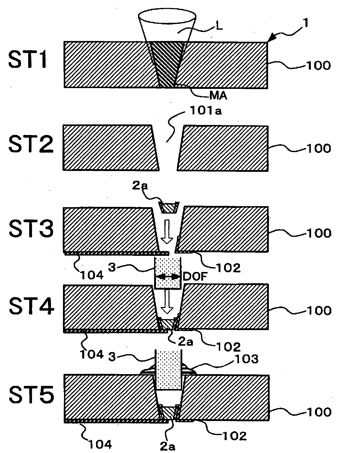
[0048] A first embodiment of the present invention relates to an example in which an optical device and an optical fiber are mounted inside a tapered through-hole with one end open thereof.

[0049] FIG. 1 shows cross-sectional views of the manufacturing steps illustrating a manufacturing method of an optical communication module according to a first embodiment. Although FIG. 1 shows expanded cross-sectional views with respect to one through-hole, cases where a plurality of through-holes is formed on one substrate can be considered similarly.

[0050] Tapered Through-hole Forming Step: ST1

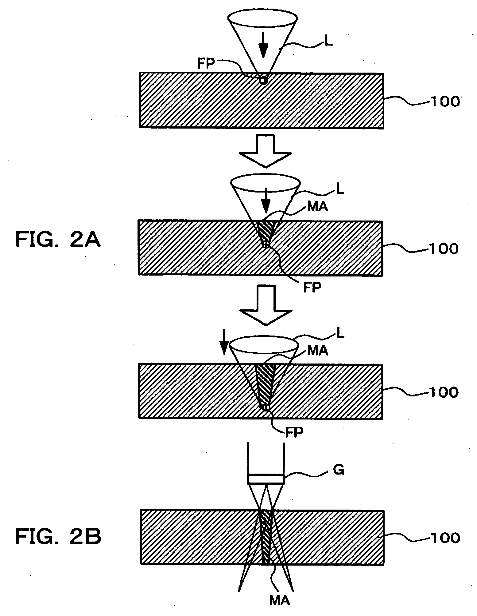
[0051] First, a tapered through-hole 101a is provided in a substrate 100. As for the substrate 100, although a substrate with or without a light-transmitting property may be used, a material, for which piercing work is easy and which does not cause deformation and subsequent displacement after manufacturing the optical communication module, is suitable. Particularly, in the present embodiment, a femto-se...

second embodiment

[0090] According to a second embodiment of the present invention, another optical device is further housed in one through-hole before housing an optical fiber. FIG. 5 shows cross-sectional views of manufacturing steps illustrating a manufacturing method of an optical communication module according to the second embodiment of the present invention.

[0091] The present embodiment is similar to the first embodiment except for mounting of another optical device 4. Accordingly, the forming step of the tapered through-hole 101a corresponds to ST1 and ST2 of FIG. 1, the mounting step of the optical device 2a (ST11) corresponds to ST3 of FIG. 1, the mounting step of the optical fiber 3 (ST13) corresponds to ST4 of FIG. 1, and the fixing step (ST14) corresponds to ST5 of FIG. 1. Therefore, the same members and shapes as those of the first embodiment are indicated by the same numerals and signs and their description will be omitted.

[0092] However, according to the present embodiment, because th...

third embodiment

[0106] A third embodiment of the present invention relates to an optical communication module using a double-ended tapered through-hole (hour-glass shaped), which is opened bi-directionally.

[0107] FIG. 7 shows cross-sectional views of the manufacturing steps illustrating a manufacturing method of an optical communication module according to the third embodiment of the present invention. Although FIG. 7 shows expanded cross-sectional views of one through-hole, a case where a plurality of through-holes is formed in one substrate can be considered similarly. The same members and shapes as those of the first embodiment are indicated by the same numerals and signs, and their description will be omitted.

[0108] Tapered Through-hole Forming Step: ST21

[0109] Firstly, a double-ended tapered through-hole 101b is provided in the substrate 100. The substrate 100 and the femto-second pulse laser are similar to those of the above-described first embodiment. However, irradiation conditions of the l...


PUM


Abstract

A method is provided to precisely mount an optical device and an optical fiber without manual alignment. A tapered through-hole is provided in a substrate to house the optical device whose optical transmission point substantially coincides with a geometrical center. The optical transmitter having a larger diameter than a diameter of the optical device is further inserted in the tapered through-hole housing the optical device.

Description

[0001] The present application claims priority to Japanese Patent Application No. 2003-064136 filed Mar. 10, 2003 which is hereby expressly incorporated by reference herein in its entirety.[0002] 1. Field of the Invention[0003] The present invention relates to a manufacturing method of an optical communication module, and particularly to a structure and a manufacturing method of the optical communication module, which couples an optical device to an optical fiber while preferably aligning them on a substrate.[0004] 2. Description of Related Art[0005] An optical communication module couples an optical device such as a surface emitting laser and a photo-detector, which mutually convert an electrical signal and an optical signal via optical fiber. The optical communication module has attracted attention as a transmission means for communicating a large amount of information.[0006] Conventionally, as for the optical coupling between an optical device and an optical fiber in a direction ...

Claims


Application Information

Patent Timeline
IPC IPC(8): G02B6/42
CPCG02B6/4201G02B6/4228G02B6/424G02B6/4244G02B6/4245G02B6/4257
Inventor FUJII, EIICHIKOYAMA, TOMOKO
Owner SEIKO EPSON CORP
Why Eureka
Try Eureka