Built-in self test circuit

a self-testing, circuit technology, applied in the direction of solid-state devices, instruments, semiconductor devices, etc., can solve the problems of large number of test patterns, large test time, and large cost of circuit test using the above scan paths

Inactive Publication Date: 2003-10-09
RENESAS ELECTRONICS CORP
View PDF20 Cites 20 Cited by
  • Summary
  • Abstract
  • Description
  • Claims
  • Application Information

AI Technical Summary

Benefits of technology

[0016] In accordance with the BIST circuit and the method of the present invention, since the test patterns to be generated by the verification test pattern generator in the BIST circuit are used for verification of design connections in the LSI during the design stage thereof, man-hours for creating the verification test patterns can be reduced. In addition, since the number of test patterns to be generated by the verification test pattern generator can be much smaller than the number of test patterns to be generated by the conventional test pattern generator due to the limited usage thereof, the time length needed to verify the design connections in the LSI can be reasonably short.

Problems solved by technology

The circuit test using the above scan paths costs a large amount of time due to the configuration wherein the serially connected flip-flops consecutively shift the scan-in signal responding to the clock signal.
However, since the ordinary test patterns generated by the test pattern generator are dedicated to finding the physical defects in the LSI, the number of test patterns is large.
Thus, if the ordinary test patterns are used for verifying the LSI in the design stage thereof, the verification necessitates a larger amount of test time.
In addition, if the verification test patterns for use in the design verification are manually created separately from the ordinary test patterns to be generated by the BIST circuit, this costs huge man-hours to thereby raise the fabrication costs of the LSI.
In addition, since the number of test patterns to be generated by the verification test pattern generator can be much smaller than the number of test patterns to be generated by the conventional test pattern generator due to the limited usage thereof, the time length needed to verify the design connections in the LSI can be reasonably short.

Method used


Image

  • Built-in self test circuit
  • Built-in self test circuit
  • Built-in self test circuit

Examples


Embodiment Construction

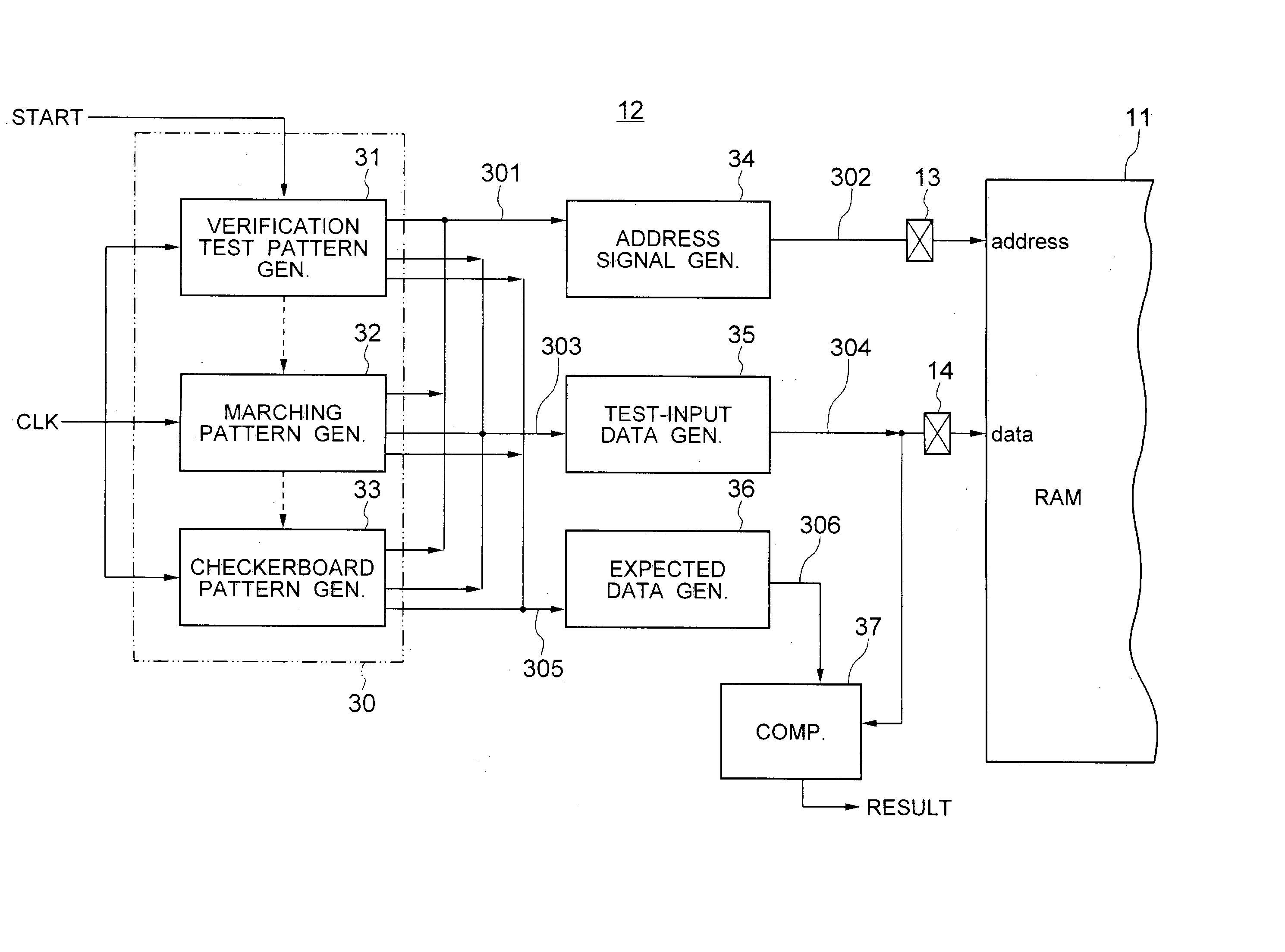
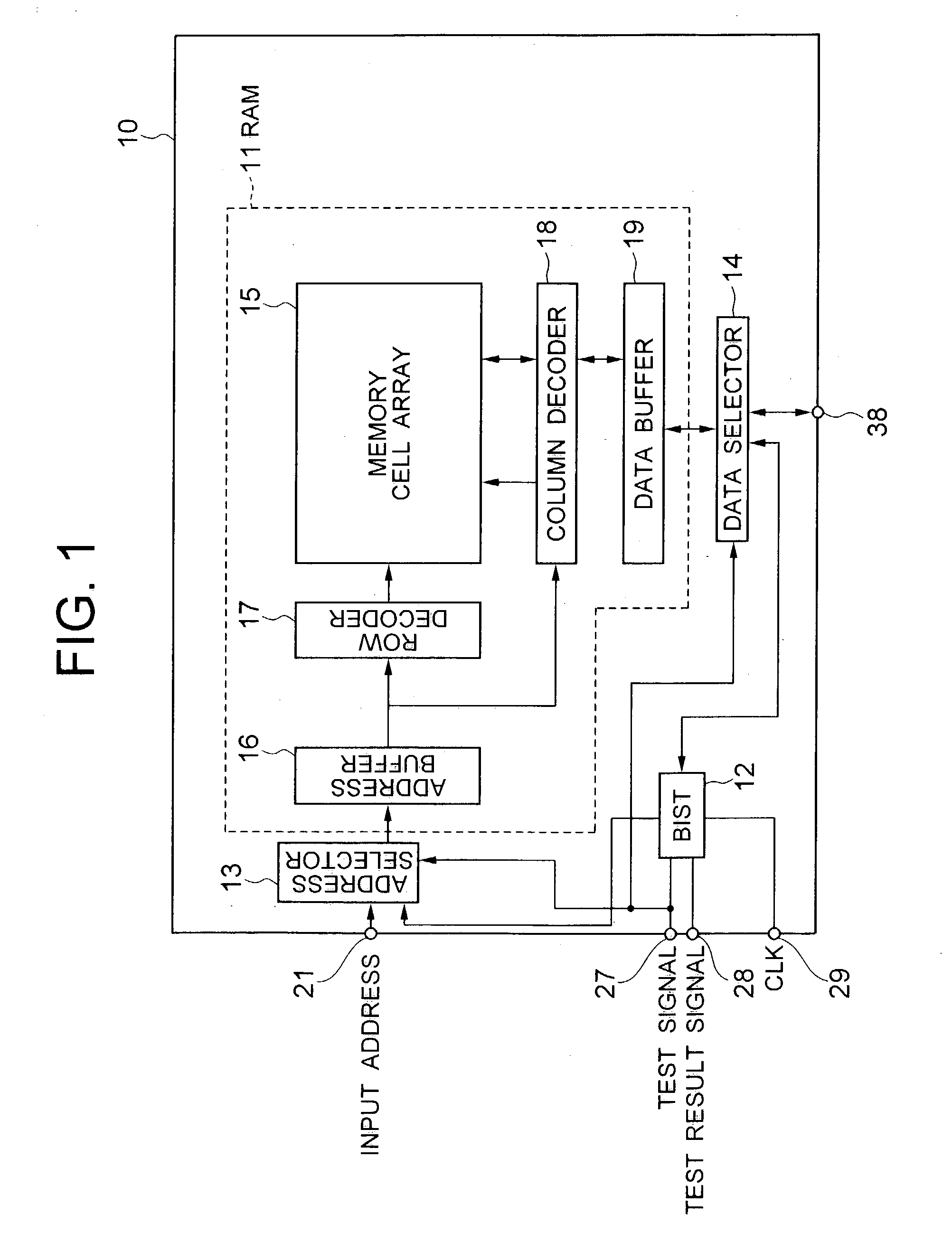
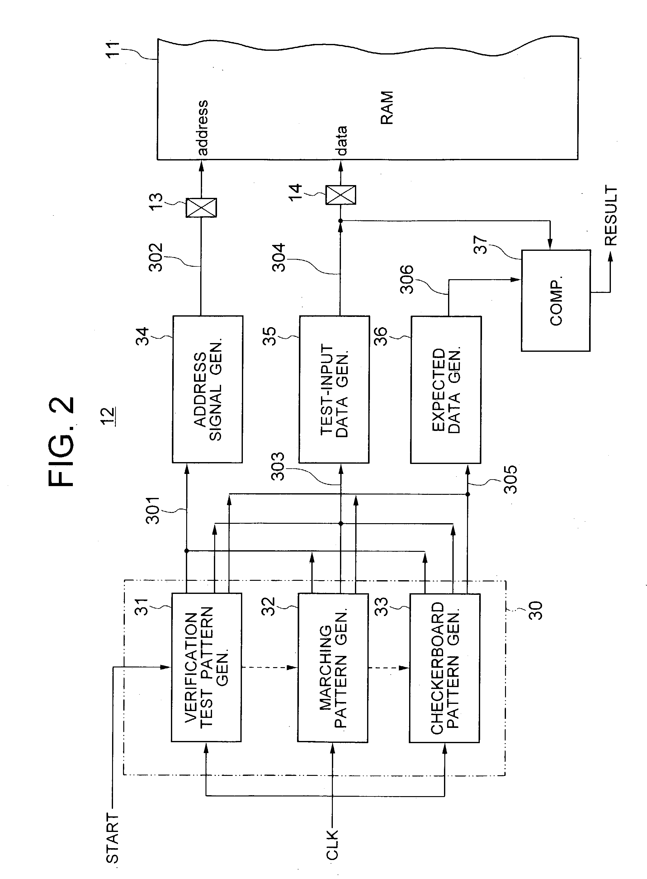
[0028] The BIST circuit according to the present invention is preferably incorporated in an LSI including a logic circuit and / or memory device, such as system LSI, logic LSI and DRAM.

[0029] If the BIST circuit according to the present invention is incorporated in a logic LSI or logic core block, for example, another BIST circuit is preferably incorporated therein including a test pattern generator which generates a scan-in test pattern and a scan-out data expected pattern for conducting a scan path test. The scan path test is generally used for examining the presence or absence of a physical defect in the LSI during a product test. The physical defect may arise due to an incomplete fabrication step such as in a diffusion step or etching step in the fabrication process of the LSI. For detecting the physical defect, the verification test pattern may be used in the product test while assisting the scan path test.

[0030] The design verification test pattern is preferably described in a b...


PUM


Abstract

A built-in self test circuit (BIST circuit) in an LSI includes a verification test pattern generator for generating verification test pattern which is used for verifying the connections in the LSI including the BIST circuit in the design stage thereof, and another test pattern generator which is used to test the function of the LSI.

Description

[0001] (a) Field of the Invention[0002] The present invention relates to a built-in self test (BIST) circuit, and more particularly, to a BIST circuit which is capable of generating a test pattern including series of test input signals and test result signals.[0003] (b) Description of the Related Art[0004] A BIST circuit is incorporated in an LSI for testing the function of the LSI. The LSI is evaluated by the BIST circuit as to non-defectiveness in the function thereof after the completion of the product. FIG. 10 shows a conventional BIST circuit incorporated in a system LSI (logic circuit), described in Patent Publication JP-A-8-15382.[0005] A plurality of scan paths 62 are formed each grouping the flip-flops disposed in the internal circuit of the LSI 61, when a test mode is selected for the LSI. Each scan path 62 connects the group of flip-flops in a cascade (serial) connection, and is associated with a corresponding scan-in pin 65 which receives a series of input scan-in signal...

Claims


Application Information

Patent Timeline
Patent Type & Authority Applications(United States)
IPC IPC(8): G01R31/3181G01R31/28G01R31/3183G01R31/3185G01R31/3187G11C29/10G11C29/12H01L21/822H01L27/04
CPCG01R31/31813G01R31/3187G01R31/318547
Inventor NAKAMURA, YOSHIYUKI
Owner RENESAS ELECTRONICS CORP
Why Eureka
Try Eureka