Electronic device, element substrate, electro-optical device, method of producing the electro-optical device, and electronic apparatus

a technology of electro-optical devices and elements, applied in the direction of static indicating devices, identification means, instruments, etc., can solve the problems of restricting the reduction of reducing the display quality of the electro-optical devi

Active Publication Date: 2004-11-25
SEIKO EPSON CORP
View PDF11 Cites 37 Cited by
  • Summary
  • Abstract
  • Description
  • Claims
  • Application Information

AI Technical Summary

Problems solved by technology

However, in the related art electro-optical device, due to manufacturing variations occurring in, for example, the organic EL elements that make up the respective pixels, display quality of the electro-optical device may be reduced.
Therefore, the display quality of the electro-optical device is reduced.
Therefore, it is possible to restrict a reduction in the display quality of the electro-optical device caused by a defect occurring in the control electronic element.
Accordingly, since the electro-optical material placement area that does not operate is virtually unused, it is possible to restrict a reduction in the display quality of the electro-optical device.
As a result, it is possible to provide an electro-optical device whose reduction in display quality is restricted.

Method used


Image

  • Electronic device, element substrate, electro-optical device, method of producing the electro-optical device, and electronic apparatus
  • Electronic device, element substrate, electro-optical device, method of producing the electro-optical device, and electronic apparatus
  • Electronic device, element substrate, electro-optical device, method of producing the electro-optical device, and electronic apparatus

Examples


first exemplary embodiment

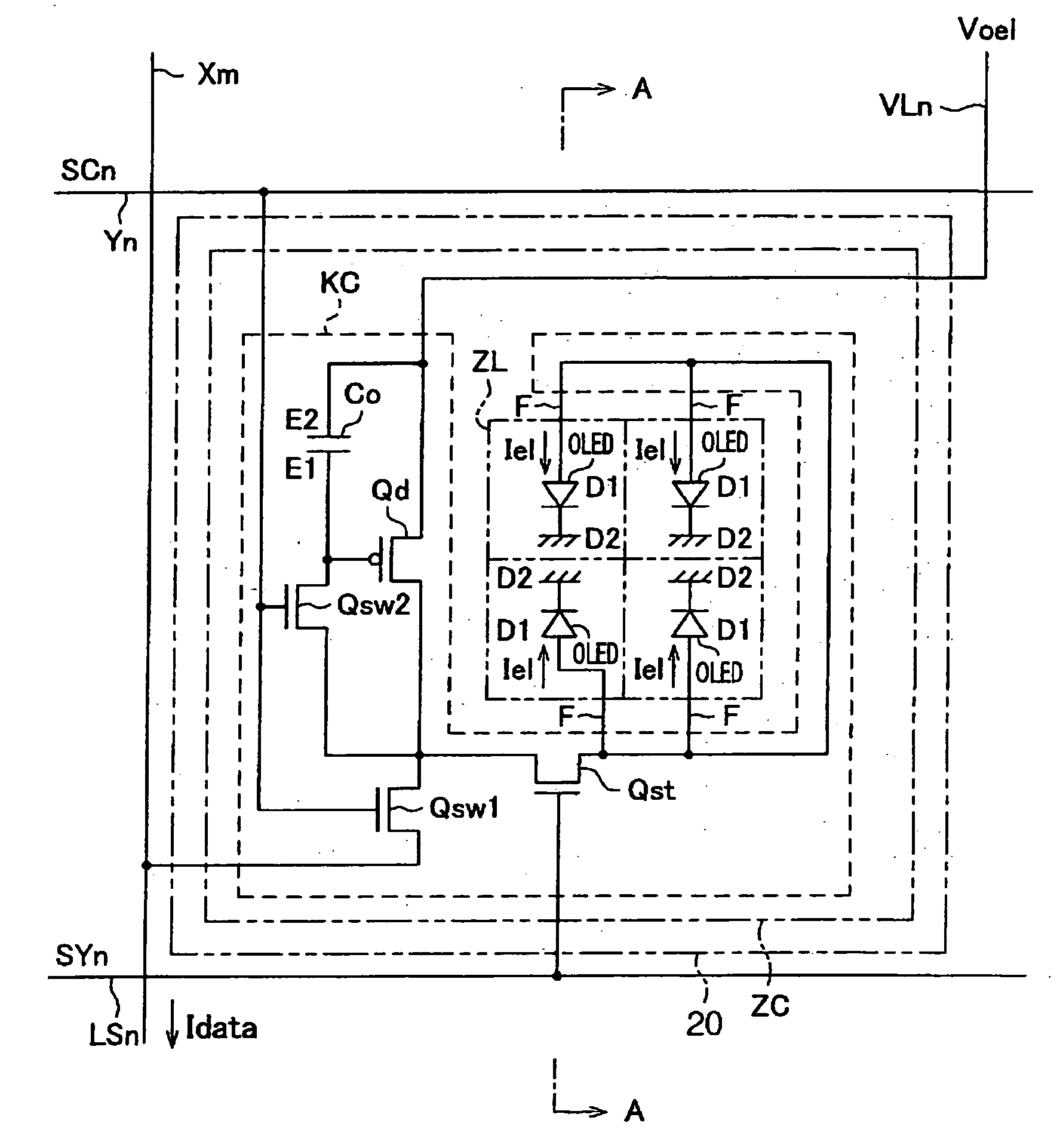
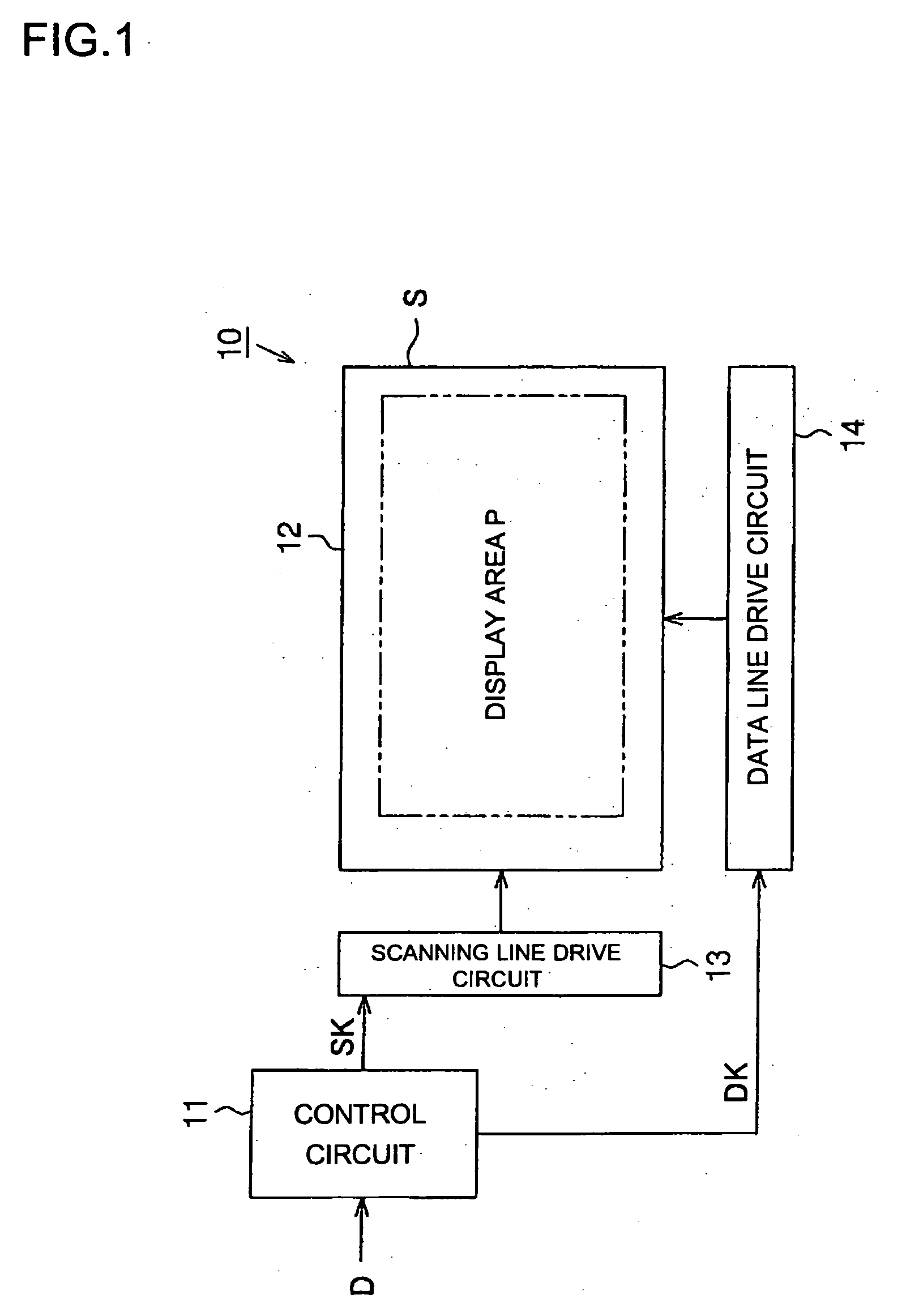
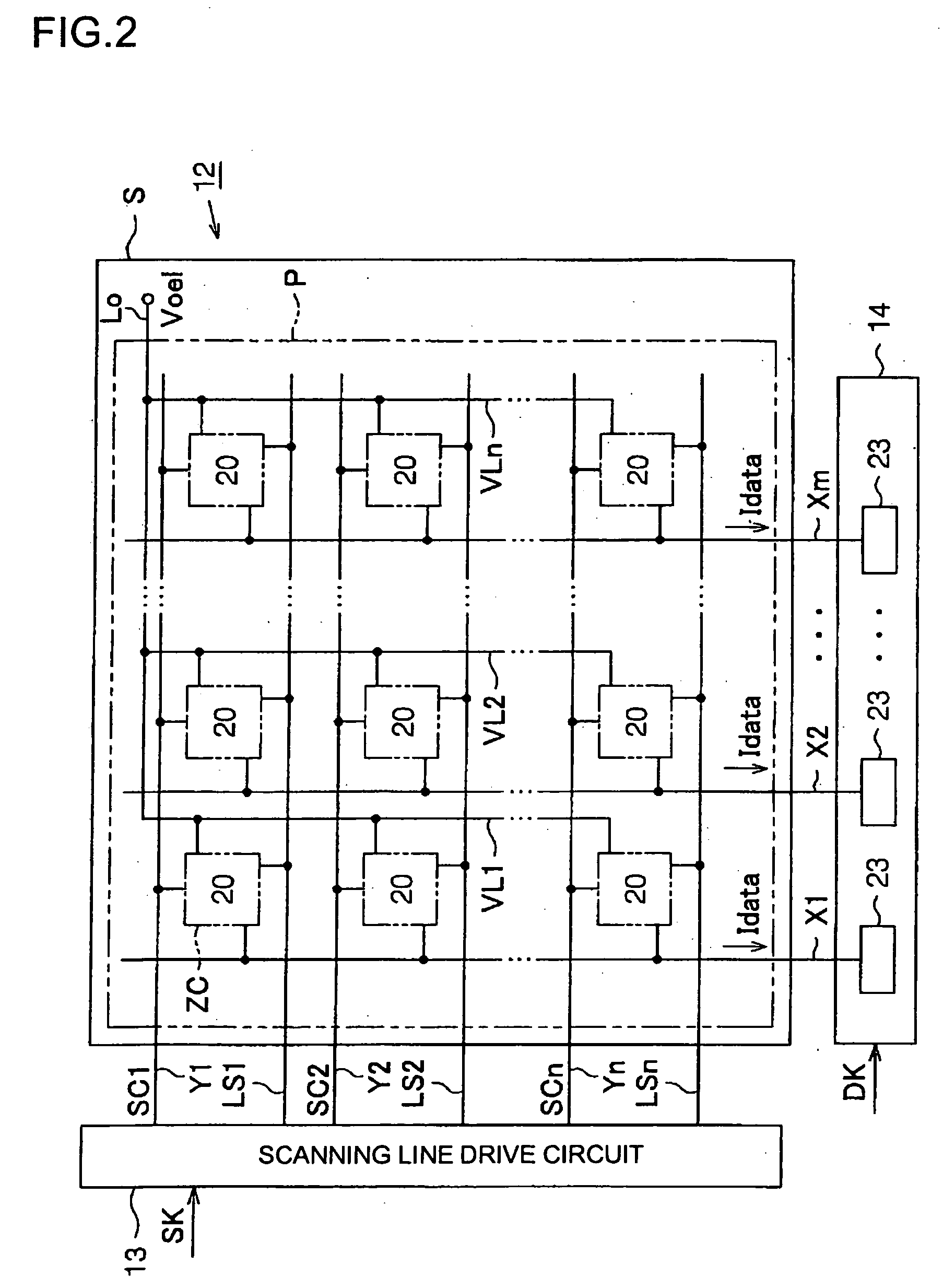
[0049] A first exemplary embodiment of the present invention will be described with reference to FIGS. 1 to 5. FIG. 1 is a block schematic of the electrical structure of an organic EL display. FIG. 2 is a block circuit schematic of the electrical structure of a display panel.

[0050] An organic EL display 10 includes a control circuit 11, a display panel 12, a scanning line drive circuit 13, and a data line drive circuit 14. The control circuit 11, the scanning line drive circuit 13, and the data line drive circuit 14 of the organic EL display 10 may be formed by individual electronic parts. For example, the control circuit 11, the scanning line drive circuit 13, and the data line drive circuit 14 may each be formed by one semiconductor integrated circuit device chip. Alternatively, all or part of the control circuit 11, the scanning line drive circuit 13, and the data line drive circuit 14, may be formed by a programmable IC chip, and the operations may be carried out using software ...

second exemplary embodiment

[0099] Next, a second exemplary embodiment of the present invention will be described with reference to FIG. 6. Structural parts in the second exemplary embodiment that correspond to those in the first exemplary embodiment are given the same reference numerals, and will not be described in detail below.

[0100] FIG. 6 shows a circuit schematic of a pixel 30 disposed in the display panel 12 of the organic EL display 10.

[0101] The locations where a circuit formation area ZC and a light emission area ZL of the pixel 30 in the exemplary embodiment are formed are not limited to the locations of the circuit formation area ZC and the light emission area ZL of each pixel 20 in the first exemplary embodiment, so that they may be disposed at any location.

[0102] The structure of the circuit of each pixel 36 in the exemplary embodiment is the same as in the first exemplary embodiment. Therefore, for convenience of explanation, the pixel 30 disposed at a location corresponding to an intersection o...

third exemplary embodiment

[0129] Next, application of the organic EL display 10 serving as an electro-optical device described in the first and second exemplary embodiments to an electronic apparatus will be described with reference to FIG. 7. The organic EL display 10 may be applied to various types of electronic apparatuses, such as a mobile personal computer, a cellular phone, and a digital camera.

[0130] FIG. 7 is a perspective view of the structure of a mobile personal computer. In FIG. 7, a personal computer 50 includes a body 52 including a keyboard 51, and a display unit 53 using the organic EL display 10.

[0131] Even in this case, the display unit 53 using the organic EL display 10 provides the same advantages as those of the first exemplary embodiment or the second exemplary embodiment. As a result, it is possible to provide the mobile personal computer 50 including the organic EL display 10 which makes it possible to perform a precise controlling operation even if a manufacturing variation occurs.

[0...


PUM


Abstract

To provide an electronic circuit, an element substrate, an electronic device, an electro-optical device, and an electronic apparatus, which make it possible to perform a precise controlling operation even if manufacturing variations occur, a circuit formation area is an annular formation area of a pixel of a display panel, and does not include a substantially central portion of the pixel. A light emission area is provided in the substantially central portion. One drive circuit is formed in the circuit formation area, and four organic elements OLED are formed in the light emission area. The drive circuit and the organic elements OLED are connected parallel to each other with wirings.

Description

[0001] 1. Field of Invention[0002] The present invention relates to an electronic device, an element substrate, an electro-optical device, a method of producing the electro-optical device, and an electronic apparatus.[0003] 2. Description of Related Art[0004] One example of a related art electro-optical device is an electro-optical device including current drive electronic elements, such as organic electroluminescence (EL) elements. In the electro-optical device, pixels including the organic EL elements are disposed in a matrix on its display panel. The pixels are connected to a data-line drive circuit through data lines. Data signals output from the data-line drive circuit are supplied to the respective pixels at a predetermined timing, and the organic EL elements emit light in accordance with current levels of the data signals. See International Publication No. WO98 / 36407 Pamphlet.[0005] However, in the related art electro-optical device, due to manufacturing variations occurring ...

Claims


Application Information

Patent Timeline
Patent Type & Authority Applications(United States)
IPC IPC(8): G09F9/00G09F9/30H05B33/10G09G3/20G09G3/30G09G3/32H01L27/32H01L51/50H05B33/00H05B33/14H05B44/00
CPCG09G3/325G09G2300/0439G09G2300/0842H01L27/3246G09G2330/08H01L27/3202H01L27/3244G09G2300/0861G09G2300/0443H10K59/84H10K59/122H10K59/12G09G3/30
Inventor JO, HIROAKI
Owner SEIKO EPSON CORP
Why Eureka
Try Eureka