Pattern forming method and system, and method of manufacturing a semiconductor device

a semiconductor integrated circuit and pattern technology, applied in the field of mask patterns, can solve the problems of not being able to increase the process margin, the pattern formation requirements are very severe, and the opc technique is not suitable for increasing the process margin

Inactive Publication Date: 2004-12-23
KK TOSHIBA
View PDF5 Cites 7 Cited by
  • Summary
  • Abstract
  • Description
  • Claims
  • Application Information

AI Technical Summary

Problems solved by technology

For this reason, the requirements for pattern formation of semiconductor integrated circuits are very severe.
For example, even if the pattern satisfies the design rule, the acute portion of the pattern is not fully transferred; as a result, it becomes round.
Thus, the OPC technique is not suitable for increasing the process margin in the lithography process.
Consequently, the OPC technique is not effective with respect to a patterns having process margin, which does not satisfy the reference value.
The foregoing pattern forming methods have a problem that it is not suitable for improving the process margin between patterns to be formed using a plurality of exposure masks.

Method used


Image

  • Pattern forming method and system, and method of manufacturing a semiconductor device
  • Pattern forming method and system, and method of manufacturing a semiconductor device
  • Pattern forming method and system, and method of manufacturing a semiconductor device

Examples


second embodiment

[0120] (Modification Example of Second Embodiment)

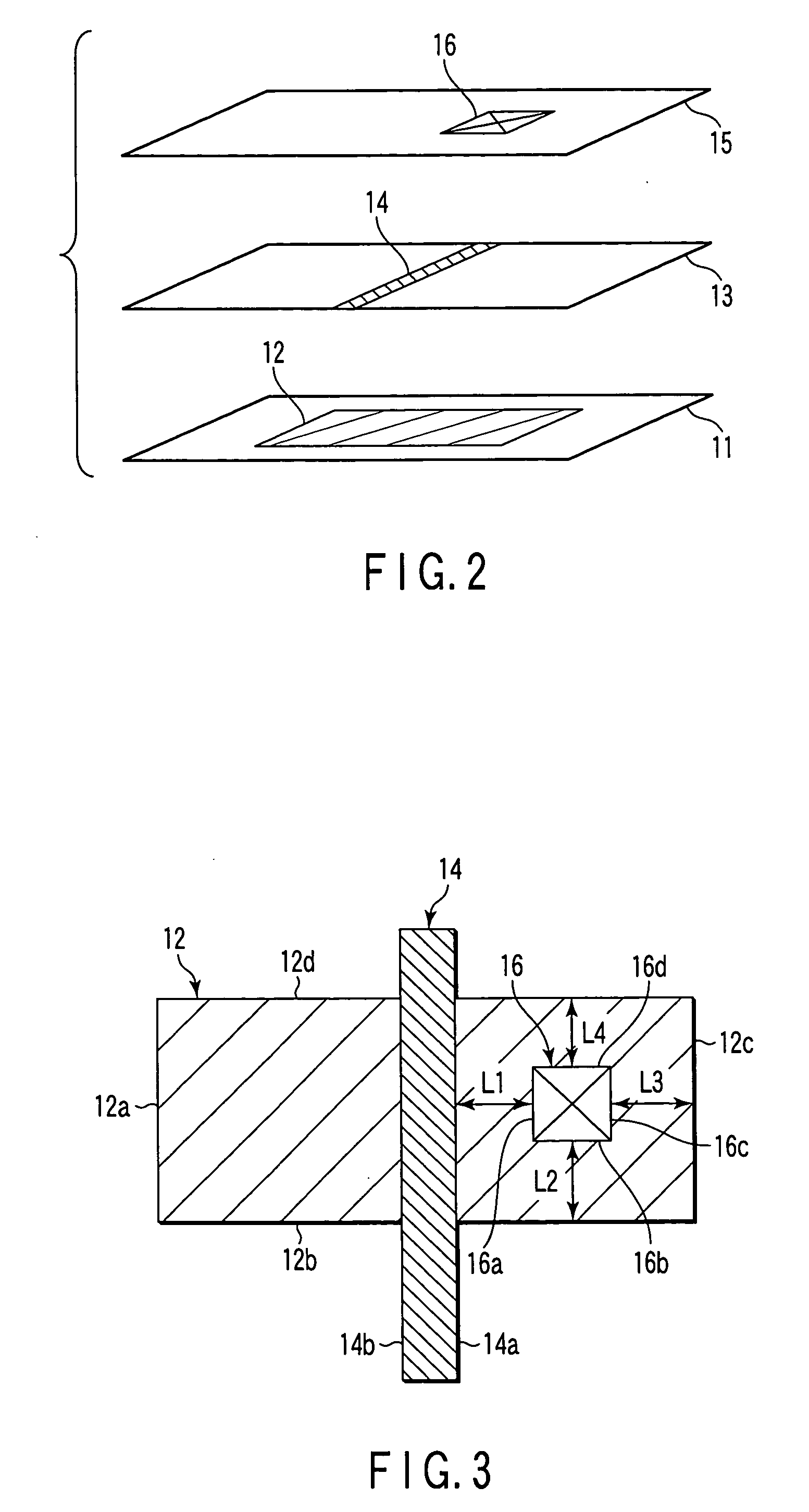
[0121] FIG. 8 shows a circuit pattern according to a second modification example of the first embodiment of the present invention. The present modification example differs from the first embodiment in that a contact hole is formed to be sandwiched by two gate wiring lines. More specifically, the second exposure mask 13 is formed with two gate patterns 34 and 38, and the third exposure mask 15 is formed with a contact hole pattern 36. According to the modification example, in order to make correspondence to the first embodiment, exposure mask formed with the gate patterns calls the second exposure mask while exposure mask formed with the contact hole pattern calls the third exposure. In this case, the given wring pattern comprises two exposure masks, and not three.

[0122] As shown in FIG. 8, the gate patterns 34 and 38 are formed at predetermined region of the semiconductor substrate formed with a gate wiring film by lithography techni...

third embodiment

[0127] (Modification Example of Third Embodiment).

[0128] FIG. 9 shows a circuit pattern according to a third modification example of the first embodiment of the present invention, in which the layout is before being corrected, and FIG. 10 shows the circuit pattern according to the third modification example of the first embodiment of the present invention, in which the layout is after being corrected. The modification example differs from the first embodiment in that two closely arranged ion implantation diffusion layer patterns are formed with contact hole patterns, respectively.

first embodiment

[0129] More specifically, the first exposure mask 11 is formed with two ion implantation diffusion layer patterns 41 and 42, and the third exposure mask 15 is formed with two contact hole patterns 46 and 47. According to the modification example, in order to make correspondence to the first embodiment, exposure mask formed with the ion implantation diffusion layer patterns calls the first exposure mask while exposure mask formed with the contact hole patterns calls the third exposure. In this case, the given wring pattern comprises two exposure masks, and not three.

[0130] As shown in FIG. 9, the two ion implantation diffusion layer patterns 41 and 42 are formed at predetermined region of the semiconductor substrate formed with a resist film by lithography technique using the first exposure mask 11, followed by ion implantation and ion activation. Thereafter, an insulating film is formed on the semiconductor substrate, and then two contact hole patterns 46 and 47 are opened in the in...


PUM

PropertyMeasurementUnit
distanceaaaaaaaaaa
dimensionsaaaaaaaaaa
widthaaaaaaaaaa

Abstract

A pattern forming method of forming a desired pattern on a semiconductor substrate is disclosed, which comprises extracting a first pattern of a layer, extracting a second pattern of one or more layers overlapped with the layer, the second pattern being arranged close to or overlapped with the first pattern, calculating a distance between the first and second patterns on a semiconductor substrate in consideration of a predetermined process variation, determining whether or not the distance between the first and second patterns satisfy an allowable margin given for the distance between the first and second patterns, and correcting, if the distance does not satisfy the allowable margin, at least one of the first and second patterns to satisfy the allowable margin.

Description

[0001] This application is based upon and claims the benefit of priority from prior Japanese Patent Application No. 2003-110254, filed Apr. 15, 2003, the entire contents of which are incorporated herein by reference.[0002] 1. Field of the Invention[0003] The present invention relates to a mask pattern. In particular, the present invention relates to a pattern forming method and system, which are suitable for forming patterns having a sufficient process margin, and to a method of manufacturing a semiconductor device using the pattern forming method.[0004] 2. Description of the Related Art[0005] Recently, high integration and high-speed performance of semiconductor devices have advanced. For this reason, the requirements for pattern formation of semiconductor integrated circuits are very severe.[0006] In semiconductor integrated circuits, the design rule representing the design and manufacture minimum line width becomes narrow with the improvement of nano-fabrication techniques. At pr...

Claims


Application Information

Patent Timeline
Patent Type & Authority Applications(United States)
IPC IPC(8): G03F1/36G03F1/68G03F1/70G03F7/00G03F7/20G03F9/00H01L21/027
CPCG03F1/144G03F7/70433G03F7/70466G03F7/705G03F1/70
Inventor NAKANO, AYAKOKOTANI, TOSHIYA
Owner KK TOSHIBA
Why Eureka
Try Eureka