Solid-state imaging device

a solid-state imaging and imaging device technology, applied in the direction of radioation control devices, instruments, television systems, etc., can solve the problems of limited spatial resolution improvement, difficult for the photoconductive layers to completely absorb light in the respective wavelength region,

Active Publication Date: 2004-12-23
SONY SEMICON SOLUTIONS CORP
View PDF3 Cites 101 Cited by
  • Summary
  • Abstract
  • Description
  • Claims
  • Application Information

AI Technical Summary

Benefits of technology

[0010] Therefore, an object of the present invention is to provide a single-plate color solid-state imaging device of a photoconductive-layer-stacked type achieving the higher color resolution and the better sensitivity.

Problems solved by technology

This results in limited improvement of the spatial resolution.
The issue here is that, in the above solid-state imaging device of a photoconductive-layer-stacked type, it is difficult for the photoconductive layers to completely absorb the light in the respective wavelength regions.

Method used


Image

  • Solid-state imaging device
  • Solid-state imaging device
  • Solid-state imaging device

Examples


Embodiment Construction

[0018] In the below, a solid-state imaging device of an embodiment of the present invention is described in detail by referring to the accompanying drawings.

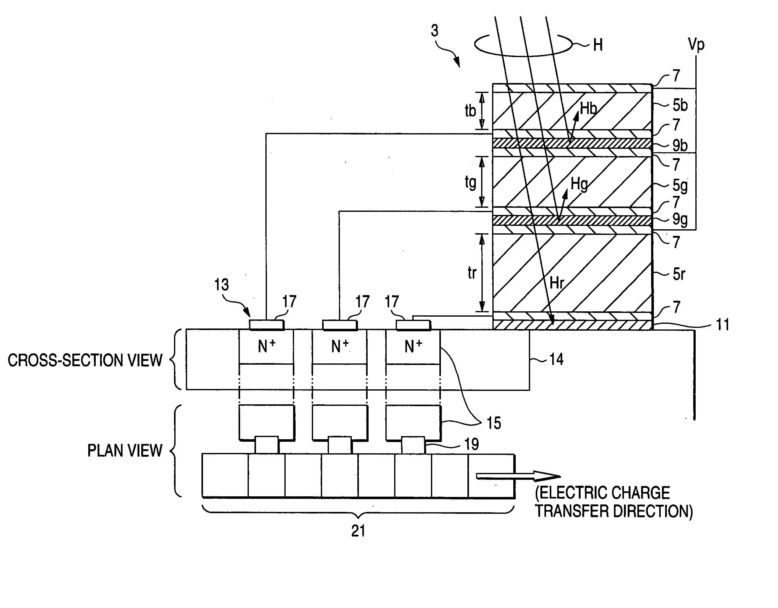
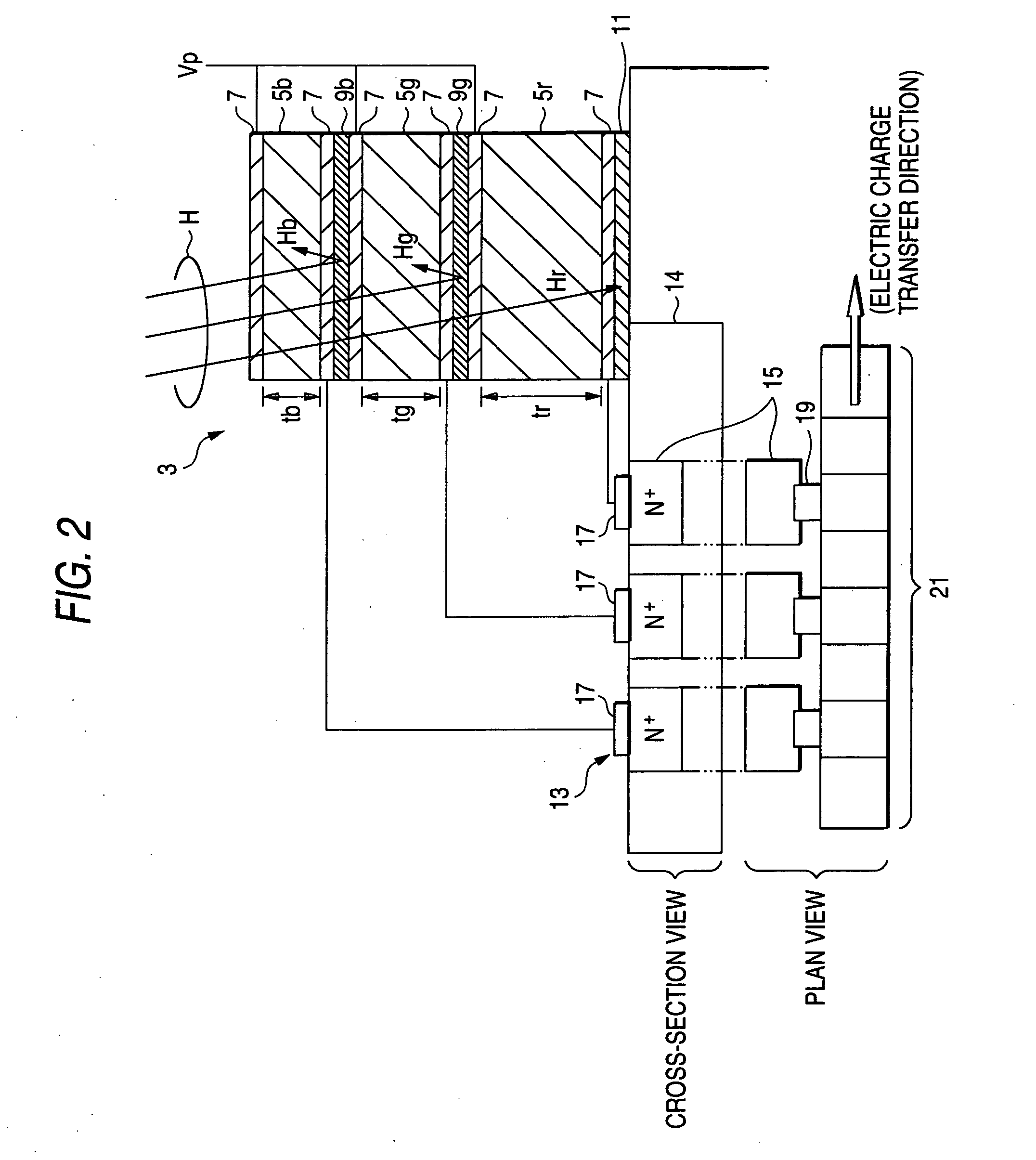
[0019] FIG. 2 is a diagram showing the main structure of an exemplary solid-state imaging device having applied with the present invention. In the drawing, the solid-state imaging device includes a substrate 1 exemplarily made of single-crystal silicon, and on the surface thereof, a plurality of pixels are arranged in matrix (in the drawing, only one pixel is shown). On each of the pixels, a light receiving section 3 is provided.

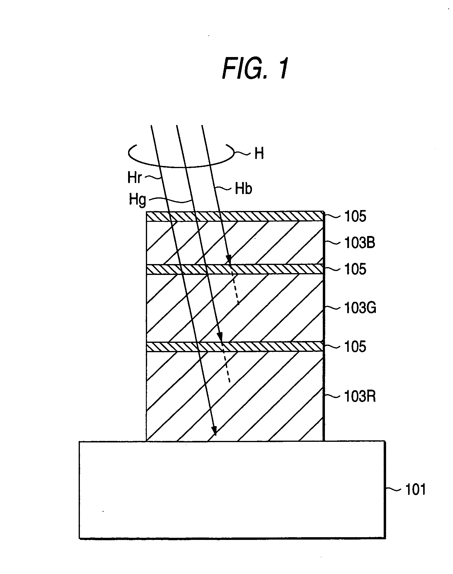
[0020] The light receiving section 3 includes a photoconductive layer 5r for red, a photoconductive layer 5g for green, and a photoconductive layer 5b for blue, those of which are stacked in this order on the substrate 1. A transparent electrode layer 7 is provided above and below of each of these photoconductive layers 5r, 5g, and 5b. That is, the photoconductive layer 5r is sandwiched between the trans...


PUM


Abstract

A solid-state imaging device including a substrate corresponding to a pixel. The substrate carries thereon a light receiving section, which is a stack of, in this order, a photoconductive layer for absorbing light in a wavelength region for red, a photoconductive layer for absorbing light in a wavelength region for green, and a photoconductive layer for absorbing light in a wavelength region for blue. A transparent electrode layer is provided on each of the photoconductive layers. The transparent electrode layer placed above the photoconductive layer and the transparent electrode layer placed below the photoconductive layer are sandwiching a translucent reflective layer for reflecting the light in the green wavelength region. Similarly, a translucent reflective layer is sandwiched between the transparent electrode layer placed above the photoconductive layer and the transparent electrode layer placed below the photoconductive layer for reflecting the light in the blue wavelength region. With such a structure, successfully provided is a single-plate color solid-state imaging device of a photoconductive-layer-stacked type achieving the higher color resolution and the better sensitivity.

Description

[0001] 1. Field of the Invention[0002] The present invention relates to single-plate color CCD and CMOS solid-state imaging devices and, more specifically, to a solid-state imaging device of a photoconductive-layer-stacked type, including a stack of photoconductive layers serving as an optical-electrical conversion section on a substrate.[0003] 2. Description of the Related Art[0004] In a single-plate color solid-state imaging device of a general type, color filters such as R (Red), G (Green), and B (Blue) are assigned to a pixel formed with a light receiving section. With the solid-state imaging device structured as such, the pixels each assigned with various color filters are put in groups to derive a color signal. This results in limited improvement of the spatial resolution. For betterment, recently proposed is a solid-state imaging device including a stack of photoconductive layers (optical-electrical conversion layers) serving as an optical-electrical conversion section with a...

Claims


Application Information

Patent Timeline
Patent Type & Authority Applications(United States)
IPC IPC(8): G03G15/04H01L27/146H01L31/0216H01L31/10H04N5/335H04N5/369H04N5/372H04N5/374
CPCH01L27/14621H01L27/14647H01L31/02165A63H33/108
Inventor KANBE, HIDEO
Owner SONY SEMICON SOLUTIONS CORP
Why Eureka
Try Eureka