Self-testing printed circuit board comprising electrically programmable three-dimensional memory

a printed circuit board and self-testing technology, applied in the field of integrated circuits, can solve the problems of high cost, high cost, and high cost of three-dimensional integration of three-dimensional blocks, and achieve the effects of improving speed and programmability, speed, yield and software upgradability, and improving data security

Inactive Publication Date: 2004-12-30
ZHANG GUOBIAO
View PDF8 Cites 10 Cited by
  • Summary
  • Abstract
  • Description
  • Claims
  • Application Information

AI Technical Summary

Benefits of technology

0022] It is a principle object of the present invention to provide an integrated circuit (IC) with self-test and at-speed test capabilities.
0023] It is a further object of the present invention to provide an IC self-test based on electrically programmable three-dimensional memory (EP-3DM).
0024] It is a further object of the present invention to provide an IC self-test method with minimum impact to the layout of the circuit-under-test.
0025] In accordance with these and other objects of the present invention, an EP-3DM-based IC self-test is disclosed.
0026] Compared with conventional memory, one greatest advantage of the 3D-M is its integratibility. Because its memory cells do not occupy substrate, most substrate real estate can be used to build complex substrate integrated circuits (substrate-IC). The substrate-IC may comprise conventional memory block, processing unit, analog block and others. 3D-M SoC (system-on-a-chip) formed from the integration between the 3D-M and substrate-IC is referred in the present invention as three-dimensional integrated memory (3DiM). The 3DiM can further improve the data security, speed, yield and software upgradibility of the 3D-M.
0027] In a 3DiM, the substrate-IC may comprise an embedded read-write memory (eRWM) and / or an embedded processor (eP). The performance of the 3D-M and the eRWM are complementary to each other: 3D-M excels in integratibility and density / cost; RWM is better in speed and programmability. The integration of the 3D-M and the RWM combines their individual strength and can achieve an optimized system performance. On the other hand, the integration of the 3D-M and the eP can enable the on-chip processing of the 3D-M data (data stored in the 3D-M), thus improving the 3D-M data security.

Problems solved by technology

Because logic and analog blocks are sensitive to defects and non-single-crystalline semiconductor material has a large defect density, the 3D-IC comprising logic and / or analog blocks have a low yield.
Moreover, logic and / or analog blocks consume large power.
The three-dimension integration of these blocks faces many heat-dissipation issues.
Moreover, it consumes little power.
However, because it is typically based on non-single-crystalline semiconductor, the performance of the 3D-M cell cannot yet compete with the conventional memory.

Method used


Image

  • Self-testing printed circuit board comprising electrically programmable three-dimensional memory
  • Self-testing printed circuit board comprising electrically programmable three-dimensional memory
  • Self-testing printed circuit board comprising electrically programmable three-dimensional memory

Examples


Embodiment Construction

[0076] 1. Three-Dimensional Integrated Memory (3DiM)

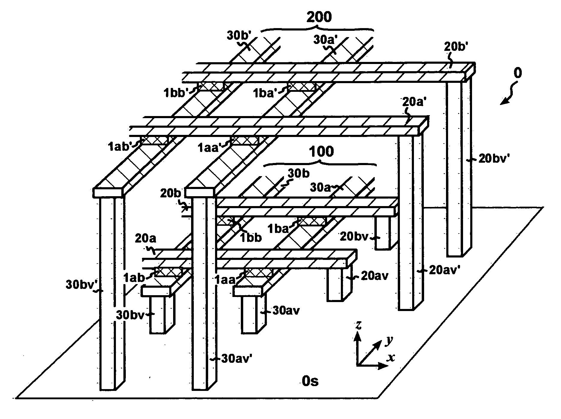
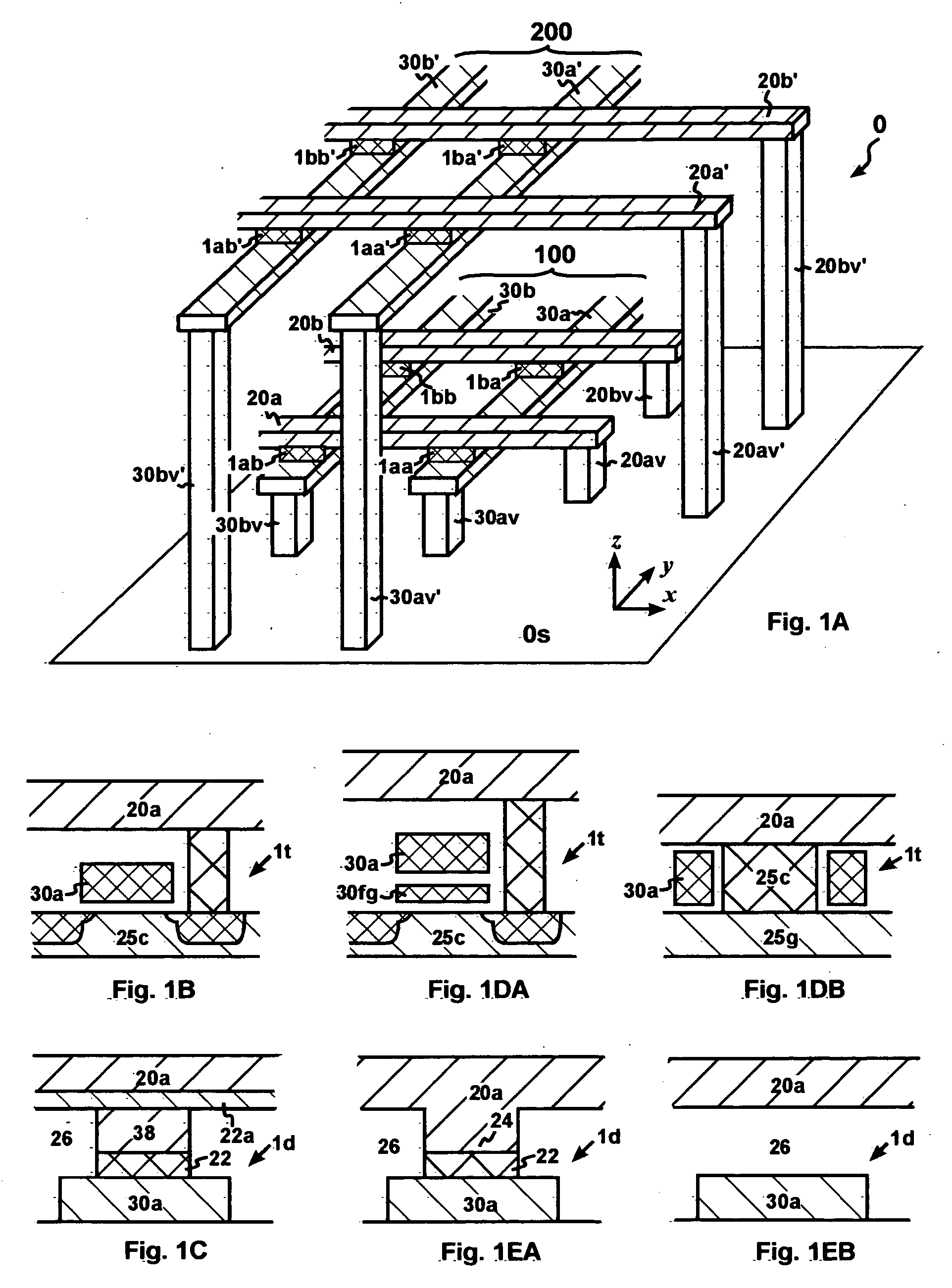
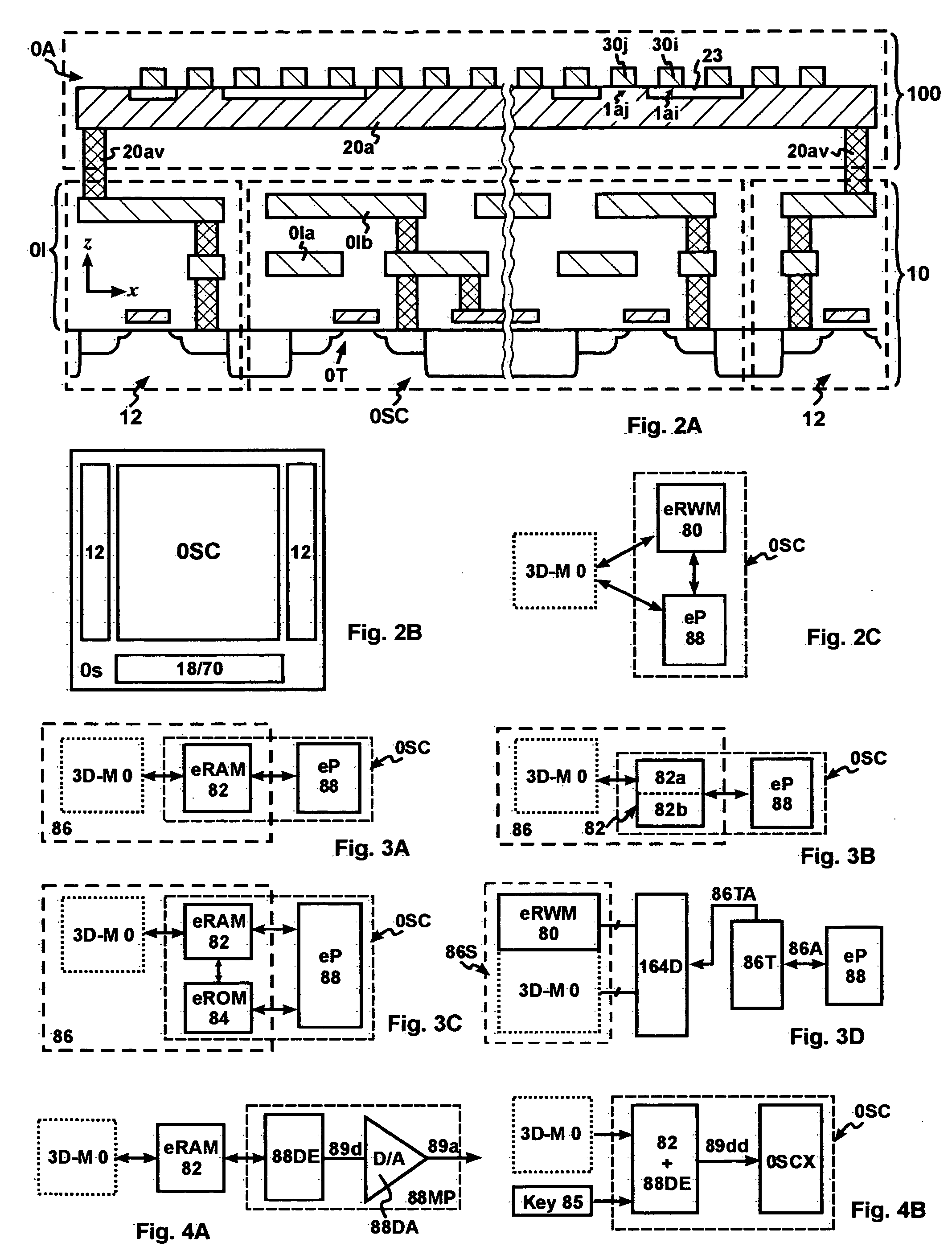
[0077] FIG. 2A is a cross-sectional view of a 3DiM. In a 3DiM, 3D-M array 0A is integrated with substrate circuit 0s 3D-M array 0A comprises one or more three-dimensional (3-D) memory level 100. Each 3-D memory level 100 comprises a plurality of address-select lines (20a, 30i . . . ) and 3D-M cells (1ai . . . ). The address-select lines comprise metallic material and / or doped semiconductor material. Transistors 0T and their interconnects (0Ia, 0Ib . . . ) form substrate circuit 0s. From a circuit perspective, substrate circuit 0s comprises a substrate-IC 0SC and address decoders 12, 18 / 70. These address decoders perform address decoding for the 3D-M array 0A. Contact vias (20av . . . ) provides electrical connection between the address-select lines (20a . . . ) and the substrate circuit 0s (e.g. address decoder).

[0078] In certain applications, the address-select lines in the 3D-M prefer to comprise poly-crystalline semiconductor (r...


PUM

PropertyMeasurementUnit
semiconductoraaaaaaaaaa
defect densityaaaaaaaaaa
poweraaaaaaaaaa

Abstract

The electrically programmable three-dimensional memory (EP-3DM) can be used to carry the test data and/or test-data seeds for the circuit-under-test (CUT). When integrated with the CUT, EP-3DM has minimum impact to the layout of the CUT. Apparently, CUT with integrated EP-3DM supports IC self-test. Moreover, with a large bandwidth with the CUT, EP-3DM-based IC self-test enables at-speed test.

Description

[0001] This is a division of Ser. No. 10 / 615,686, Filed Jul. 8, 2003, which is a division of Ser. No. 10 / 230,648, Filed Aug. 28, 2002.CROSS-REFERENCE TO RELATED APPLICATIONS[0002] This patent application relates to the following domestic patent applications:[0003] 1 "3D-ROM-Based IC Test Structure", provisional application Ser. No. 60 / 328,119, filed on Oct. 7, 2001;[0004] 2. "Three-Dimensional Read-Only Memory Integrated Circuits", provisional application Ser. No. 60 / 332,893, filed on Nov. 18, 2001;[0005] 3. "Three-Dimensional Read-Only Memory", provisional application Ser. No. 60 / 354,313, filed on Feb. 1, 2002,[0006] and the following foreign patent applications:[0007] 1. "Three-Dimensional-Memory-Based Self-Test Integrated Circuits and Methods", CHINA P. R., patent application Ser. No. 02113586.X, filed on Apr. 8, 2002;[0008] 2. "Three-dimensional Memory System-on-a-Chip", CHINA P.R., patent application Ser. No. 02113.738.2, filed on May 15, 2002,[0009] all by the same inventor.BA...

Claims


Application Information

Patent Timeline
Patent Type & Authority Applications(United States)
IPC IPC(8): G11C7/18G11C29/00H01L27/06
CPCG11C7/18G11C17/06G11C17/14H01L29/76G11C29/846H01L27/0688H01L23/58G11C29/822
Inventor ZHANG, GUOBIAO
Owner ZHANG GUOBIAO
Why Eureka
Try Eureka