Substrate for semiconductor package wire bonding method using thereof

a technology of wire bonding method and substrate, which is applied in the direction of printed circuit aspects, non-metallic protective coating applications, circuit inspection/indentification, etc., can solve the problem of difficult to make the substrate in a compact siz

Active Publication Date: 2005-01-06
AMKOR TECH SINGAPORE HLDG PTE LTD
View PDF12 Cites 26 Cited by
  • Summary
  • Abstract
  • Description
  • Claims
  • Application Information

AI Technical Summary

Benefits of technology

[0010] In an exemplary embodiment, such a substrate includes an insulative core layer, a die attachment region formed on the core layer; a plurality of electrically conductive structures, e.g., electrically conductive patterns including bond fingers, a power ring, and a ground ring, formed on the core layer outward of the die attachment region; a solder mask coated on-the core layer, and the entire outer peripheral edge of the electrically conductive patterns while exposing certain regions of the electrically conductive patterns, and one or more reference marks formed on the core layer outward of the die attachment region in such a manner that a shift state of the solder mask can be checked during a wire bonding process so that, in the connection of wire bonds to the electrically conductive patterns, the shift state of the solder mask can be compensated by adjusting the point of connection of a wire bond to the electrically conductive patterns. The reference mark may include one or more reference patterns formed on the insulative layer, typically of the same material (e.g., metal such as copper) as the elec...

Problems solved by technology

However, such an NSMD type of substrate has a problem in that, considering the tolerance of the placement of the solder mask, the bond fingers, the power ring, the gr...

Method used


Image

  • Substrate for semiconductor package wire bonding method using thereof
  • Substrate for semiconductor package wire bonding method using thereof
  • Substrate for semiconductor package wire bonding method using thereof

Examples


Embodiment Construction

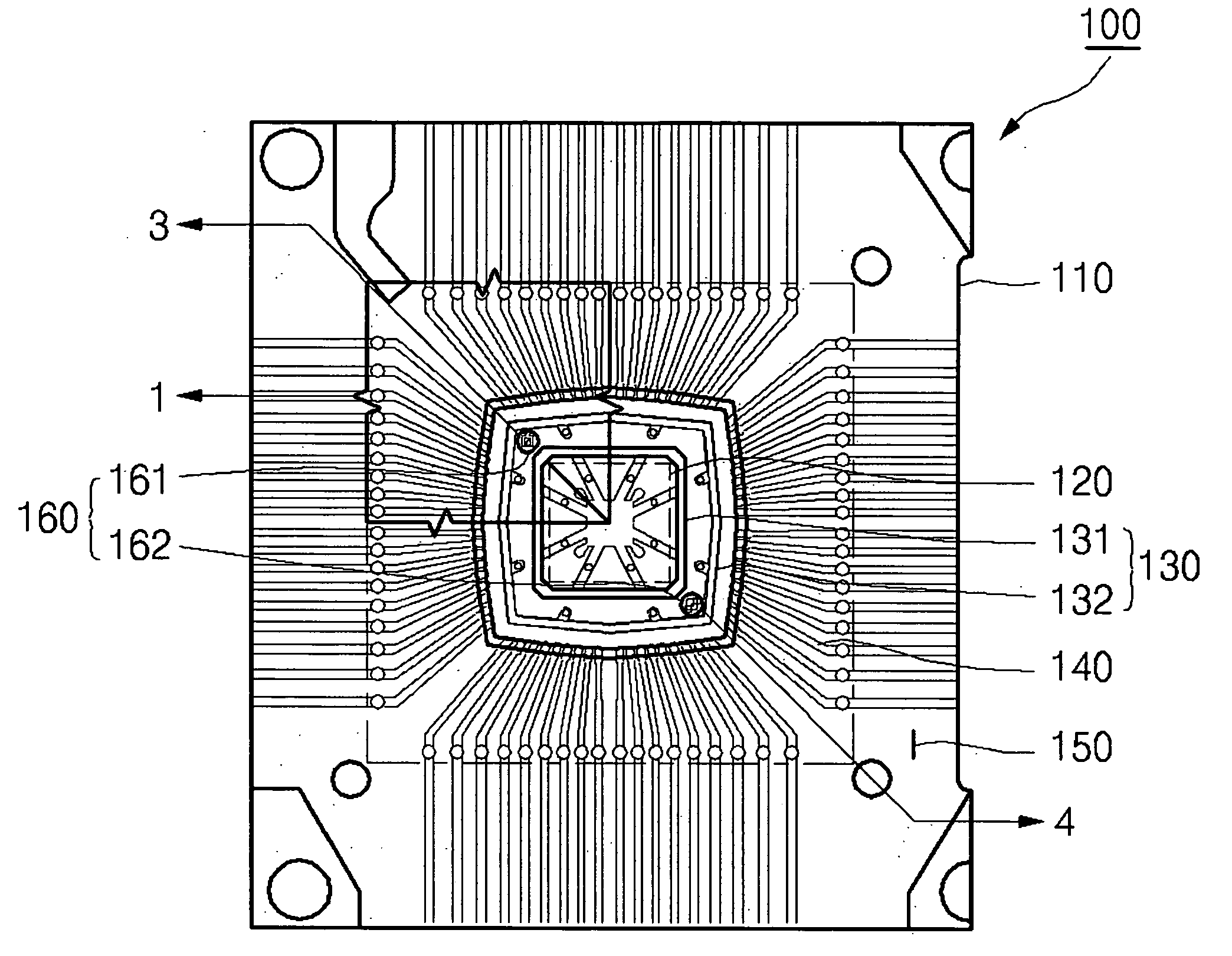
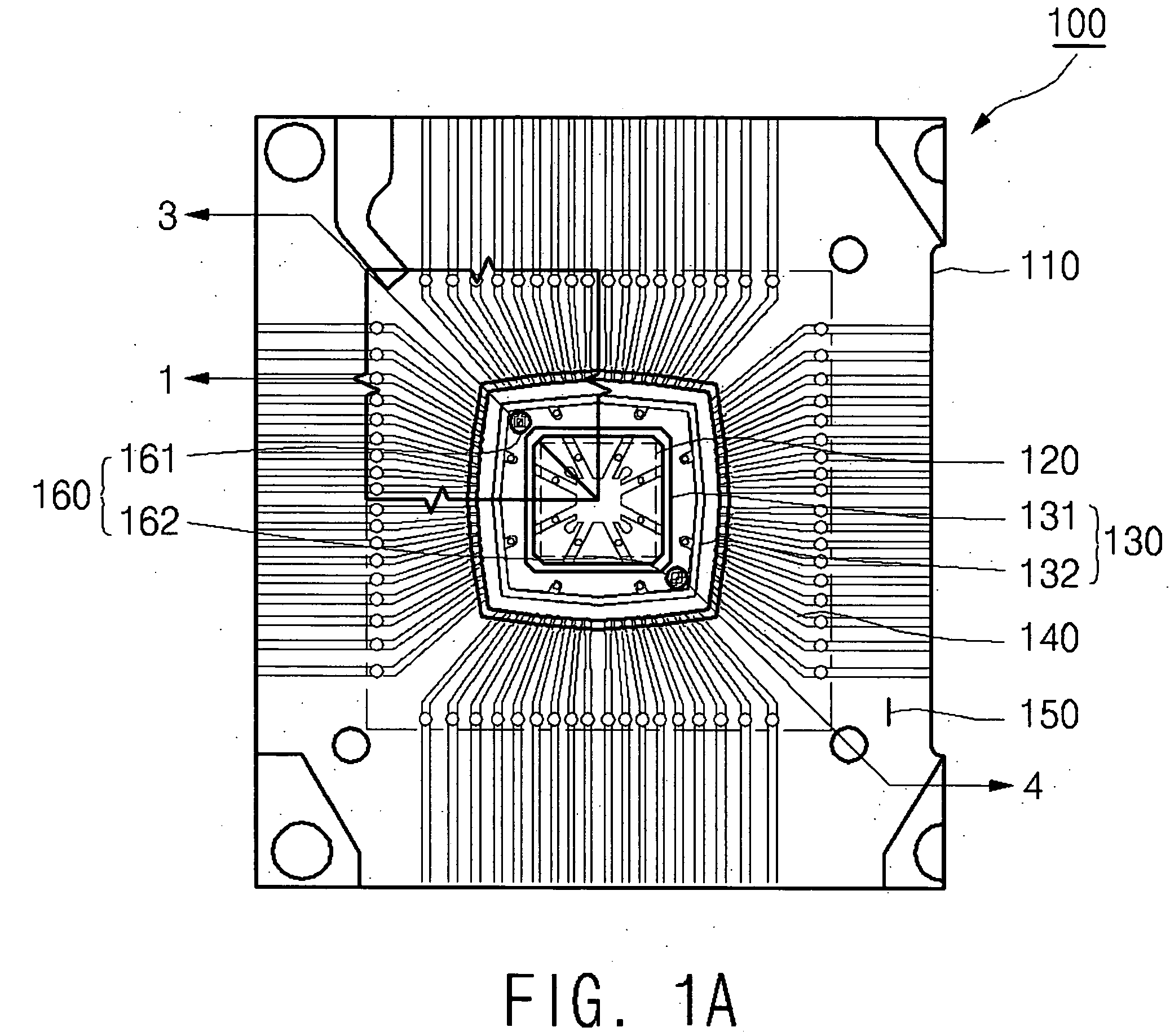
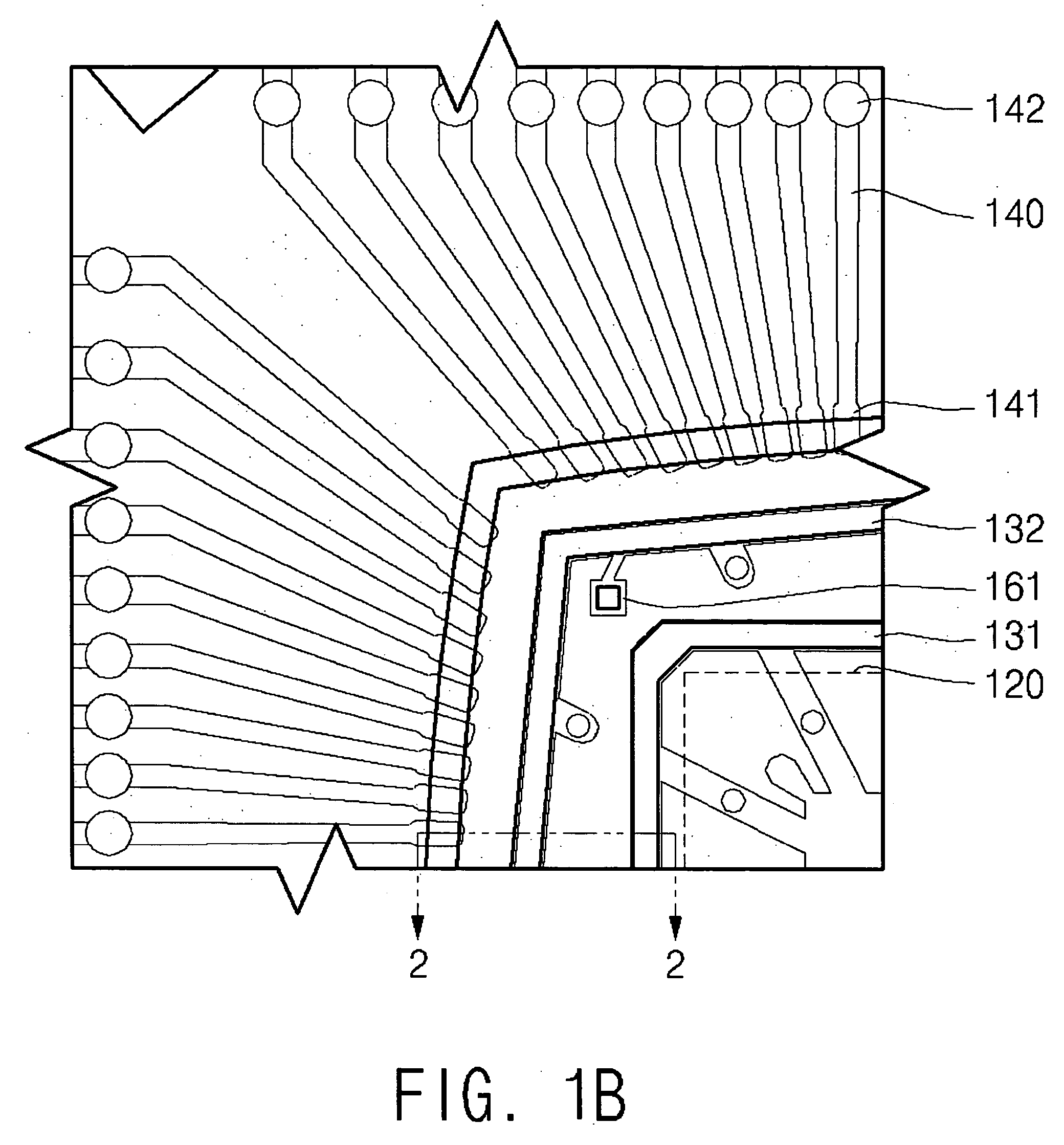
[0028] Referring to FIGS. 1A-1D, a substrate 100 for semiconductor package according to the present invention comprises: an insulative layer 110, which in this example is a resin layer 110, but could be ceramic or polyimide or the like; a die attachment region 120 formed on the resin layer 110; a plurality of electrically conductive patterns 140 formed outward of the peripheral edge of the die attachment region 120; a solder mask 150 coated on the entire outer peripheral edge of the electrically conductive patterns 140 while exposing certain regions thereof; and at least one reference mark 160 formed on the outer peripheral edge of the die attachment region 120 in such a manner that a shift state of the solder mask 150 can be checked during a wire bonding process or as part of some other process during the fabrication of the substrate or the semiconductor package. Of course, the reference mark 160 may also used to check whether the substrate 100 is loaded in a correct position or no...


PUM


Abstract

Disclosed is a substrate for semiconductor package and a wire bonding method using thereof. The substrate is provided with at least one reference mark on its surface to check a loading position and a shift state of a solder mask. The reference mark is composed of a combination of a reference pattern and a solder mask opening and is positioned in any location on an outer peripheral edge of a die attachment region. The reference mark may take various shapes. A method for checking a solder mask shift using the reference mark includes comparing a design value of the reference pattern and the solder mask opening with the reference pattern and the solder mask opening, which are formed in an actual material. After the solder mask shift is calculated, a wire bonding coordinate is newly constructed in consideration of the solder mask shift. This minimizes the wire bonding error.

Description

BACKGROUND OF THE INVENTION [0001] 1. Field of the Invention [0002] The present invention relates to a substrate for semiconductor package and a wire bonding method using thereof. [0003] 2. Description of the Related Art [0004] In general, “wire bonding” refers to a process wherein a semiconductor die, which is separately sawn from a wafer, is attached on a substrate using adhesive, and a bond pad, which is formed on the semiconductor die, is electrically connected to electrically conductive patterns, which are formed on the substrate. [0005] The wire bonding is performed using a wire bonder, which comprises a camera for recognizing the coordinates of the substrate and the semiconductor die; a PRS (pattern recognition system) for processing images recognized by the camera and calculating a changed wire bonding coordinate; and, a capillary for performing bonding in accordance with the changed wire bonding coordinate. The PRS compares pre-stored reference coordinates with actual coord...

Claims


Application Information

Patent Timeline
IPC IPC(8): H01L21/60H01L23/49H01L23/498H01L23/544H05K1/02H05K3/28
CPCH01L23/49838H01L23/544Y10S438/975H01L2224/48233H01L2924/014H01L2924/01033H01L2924/00014H01L24/48H05K2203/049H05K2201/0989H05K2201/09781H05K2201/09381H05K3/28H05K1/0269H01L2924/01079H01L24/49H01L24/85H01L2223/54426H01L2223/54473H01L2224/48091H01L2224/48227H01L2224/48228H01L2224/48465H01L2224/49H01L2224/73265H01L2224/85439H01L2224/85444H01L2224/85447H01L2924/01029H01L2924/01047H01L2224/78H01L2924/00H01L2224/45099H01L2224/05599H01L21/60
Inventor RYU, DONG SUPARK, DOO HYUNKIM, HO SEOK
Owner AMKOR TECH SINGAPORE HLDG PTE LTD
Why Eureka
Try Eureka