
MEMS devices monolithically integrated with drive and control circuitry

a technology of drive and control circuits, applied in static indicating devices, instruments, optical elements, etc., can solve problems such as incompatibility with standard cmos processes, inability to integrate, and sacrifice of the address torque generated between the yoke and the address electrod

Inactive Publication Date: 2005-01-06
II VI DELAWARE INC
View PDF22 Cites 47 Cited by
  • Summary
  • Abstract
  • Description
  • Claims
  • Application Information

AI Technical Summary

Problems solved by technology

Such integration has been difficult for a number of reasons, not least of which is the incompatibility of standard CMOS processes with some MEMS processes.
However, some of the address torque generated between the yoke and the address electrode is sacrificed compared to the first generation devices because the yoke slightly diminishes the surface area of the address electrode.
Despite the aforementioned advances, parallel plate electrostatic devices generate very low deflection torque and require very low stiffness suspension hinges.
Consequently, conventional micro-mirrors are relatively fragile and difficult to fabricate, and may therefore suffer from low yield and increased manufacturing expense.
Also, while various process techniques have been developed to ameliorate the stiction problem, the repeated physical contact between the moveable and fixed surfaces still reduces device reliability and lifetime.
High resolution SLMs have a considerable number of pixels, and thus require considerable drive and control electronics.
Some SLMs may require even more contacts, e.g. to provide feedback, further complicating the process of integrating the drive electronics.

Method used


Image

  • MEMS devices monolithically integrated with drive and control circuitry
  • MEMS devices monolithically integrated with drive and control circuitry
  • MEMS devices monolithically integrated with drive and control circuitry

Examples


Embodiment Construction

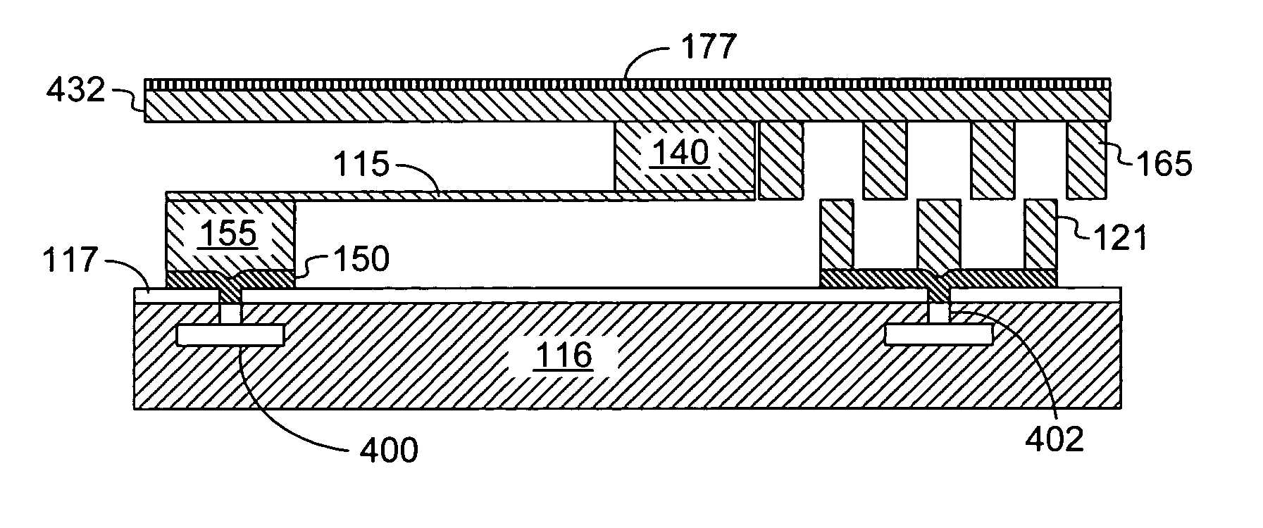
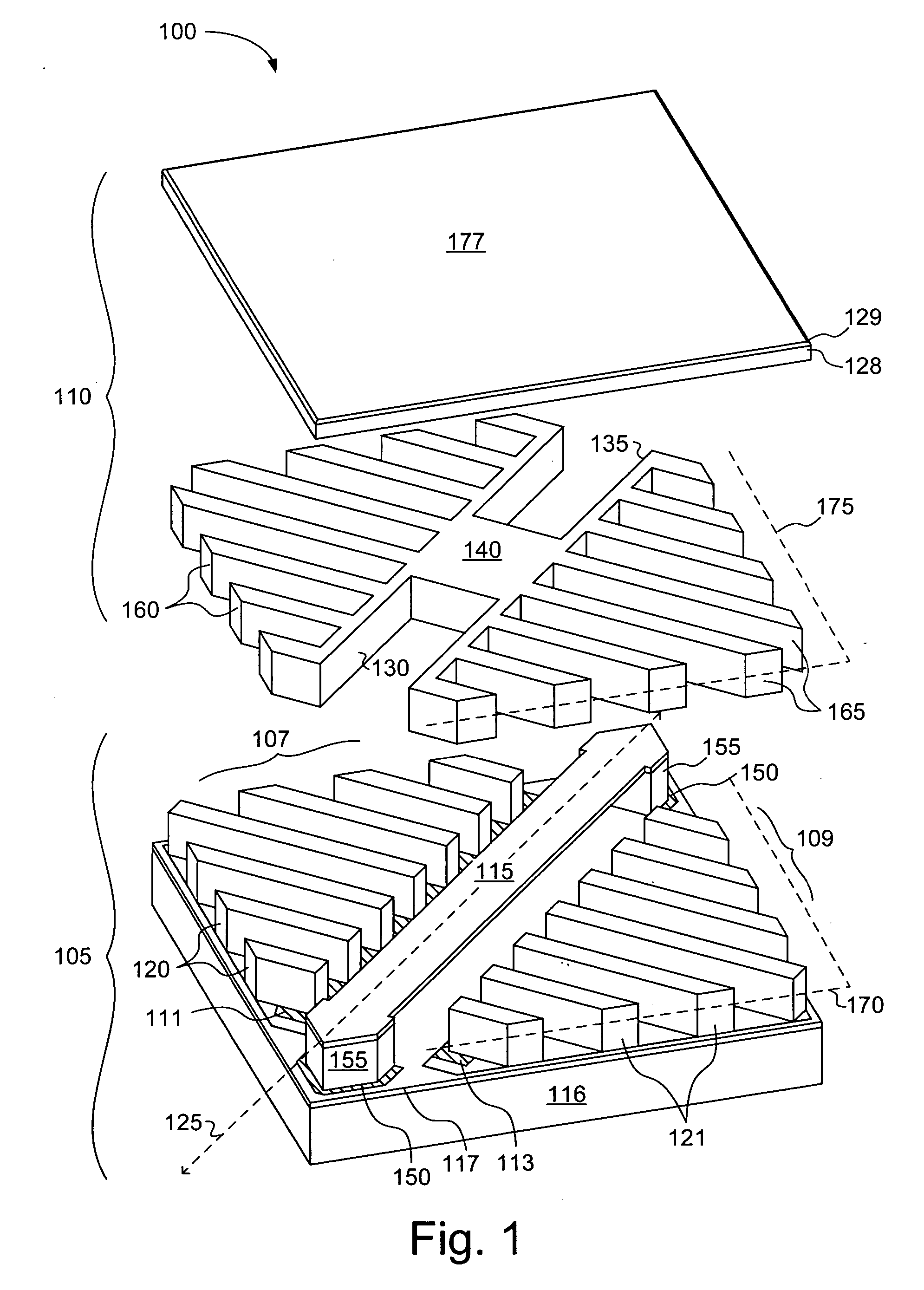
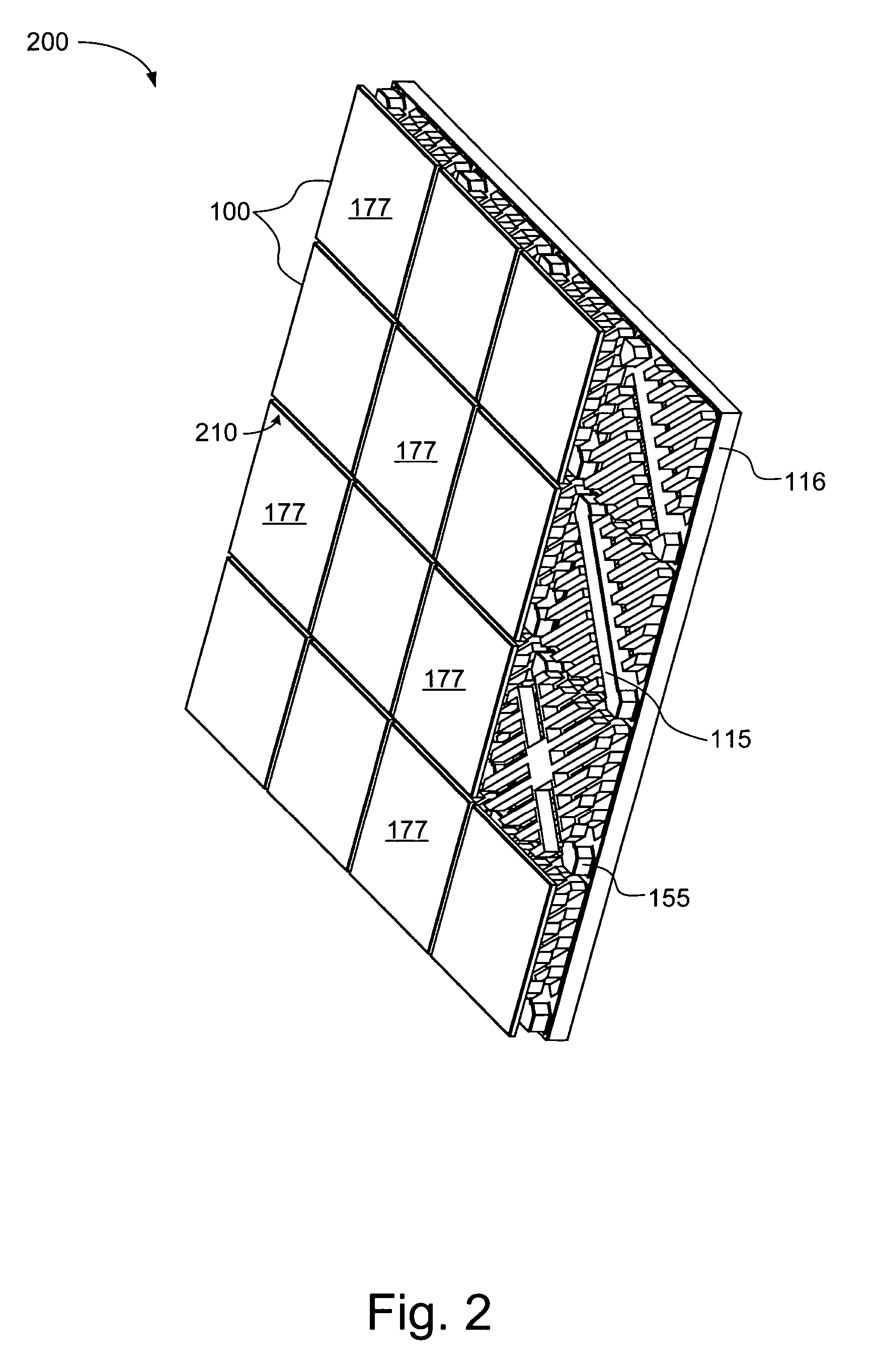
FIG. 1 depicts a Micro-Electro-Mechanical Systems (MEMS) actuator 100 in accordance with one embodiment. Actuator 100 employs hidden comb electrostatic actuators that produce much greater torque than the parallel-plate electrostatic actuators of the above-referenced Hornbeck patents. Greater torque facilitates the use of stiffer, less fragile hinge structures. Also important, comb actuators adapted for use with the invention have a more stable response curve than parallel plate actuators in the direction of deflection, and consequently afford greater position control. These and other advantages, and the means of achieving them, are detailed below.

Actuator 100 is broadly divided into a fixed (stationary) portion 105 and a movable portion 110, the two of which are interconnected via a torsional hinge 115. Fixed portion 105 includes a pair of fixed combs 107 and 109 disposed over a respective pair of addressing electrodes 111 and 113, which are in turn disposed over a substrate 116 an...


PUM


Abstract

Described are MEMS mirror arrays monolithically integrated with CMOS control electronics. The MEMS arrays include polysilicon or polysilicon-germanium components that are mechanically superior to metals used in other MEMS applications, but that require process temperatures not compatible with conventional CMOS technologies. CMOS circuits used with the polysilicon or polysilicon-germanium MEMS structures use interconnect materials that can withstand the high temperatures used during MEMS fabrication. These interconnect materials include doped polysilicon, polycides, and tungsten metal.

Description

BACKGROUND Micro Electro Mechanical Systems (MEMS) devices are being deployed in increasing numbers of applications, such as accelerometers, Radio Frequency (RF) circuits, optical micro mirrors and biotech. One of the primary requirements of modern MEMS applications is the integration of control circuitry, typically implemented in Complementary Metal Oxide Semiconductor (CMOS) technology with the MEMS structures. Such integration has been difficult for a number of reasons, not least of which is the incompatibility of standard CMOS processes with some MEMS processes. A class of MEMS devices commonly referred to as a Spatial Light Modulators (SLMs) has found numerous applications in the areas of optical information processing, projection displays, video and graphics monitors, televisions, maskless lithography, and electrophotographic printing. SLMs modulate incident light in a spatial pattern to form an image corresponding to an electrical or optical input. The incident light may be...

Claims


Application Information

Patent Timeline
IPC IPC(8): G02B26/08
CPCB81C1/00246G02B26/0841B81C2203/0735
Inventor NOVOTNY, VLAD J.SASTRI, BHARATREDDY, CHITRANJAN N.
Owner II VI DELAWARE INC
Learn More